


| Issue |
Security and Safety
Volume 5, 2026
|
|
|---|---|---|
| Article Number | 2026001 | |
| Number of page(s) | 54 | |
| Section | Integrated Circuit | |
| DOI | https://doi.org/10.1051/sands/2026001 | |
| Published online | 20 January 2026 | |
Review
A survey of post-quantum cryptographic chips: Current status, challenges, and future directions
1
School of Integrated Circuits, Tsinghua University, Beijing 100084, China
2
State Key Laboratory of Cryptography and Digital Economy Security, Beijing 100084, China
* Corresponding author (email: This email address is being protected from spambots. You need JavaScript enabled to view it.
)
Received:
29
October
2025
Revised:
29
December
2025
Accepted:
6
January
2026
Abstract
The development of quantum computing poses a serious threat to traditional cryptographic systems and has driven the rapid development of post-quantum cryptography (PQC). Specialized hardware solutions, especially PQC chips, are considered a key to achieving secure and efficient migration of quantum cryptography. This review first introduces the relevant background and the main PQC schemes and then focuses on analyzing the design challenges and bottlenecks faced by the design of PQC chips. Next, the development status and unresolved issues of different technologies, such as Central Processing Unit (CPU) Instruction-Set Extension (ISE), Field-Programmable Gate Array (FPGA), Application-Specific Integrated Circuits (ASIC), and Domain-Specific Accelerators (DSA), are further organized and analyzed. Finally, on the basis of specific application requirements, the future development technology path of PQC chips is discussed.
Key words: PQC / Cryptographic chip / Crypto-agility / ASIC / DSA
Citation: Zhu Y and Liu L. A survey of post-quantum cryptographic chips: Current status, challenges, and future directions. Security and Safety 2026; 5: 2026001. https://doi.org/10.1051/sands/2026001
© The Author(s) 2026. Published by EDP Sciences and China Science Publishing & Media Ltd.
 This is an Open Access article distributed under the terms of the Creative Commons Attribution License (https://creativecommons.org/licenses/by/4.0), which permits unrestricted use, distribution, and reproduction in any medium, provided the original work is properly cited.
1. Introduction
The advent of large-scale quantum computers [1, 2], a development that is no longer a distant possibility but an imminent technological reality, poses a serious threat to the foundations of modern digital security. For decades, the security of widely used public-key cryptographic systems, such as RSA [3] and Elliptic Curve Cryptography (ECC) [4], has been undermined by the assumed computational difficulty of classical mathematical problems, specifically integer factorization and discrete logarithms. However, in 1994, Shor [5] developed a quantum algorithm capable of solving these problems in polynomial time, making our current cryptographic infrastructure vulnerable to a quantum attack. This threat is exacerbated by the “Harvest Now, Decrypt Later” attack model [6], where adversaries are already collecting encrypted data today with the intent of decrypting them once sufficiently powerful quantum computers become available. This urgent and pervasive threat has initiated a global cryptographic transition, driving the rapid development of post-quantum cryptography (PQC), a new generation of public-key algorithms designed to be secure against both classical and quantum computers, while still being implementable on conventional semiconductor process technology.
To resist this existential challenge, multiple types of PQC algorithms have emerged, each built on a different mathematical foundation conjectured to be resistant to quantum attacks. The most prominent of these are the lattice-based algorithms [7–9], which derive their security from the computational hardness of problems in high-dimensional lattices, such as Learning With Errors (LWE) [7] and Shortest Vector Problem (SVP) [10]. Module-LWE [11] and Ring-LWE [12] problems are also proposed to provide higher efficiency, which are based on the structured lattice. This family is widely considered to be the most promising for general-purpose use, with the National Institute of Standards and Technology (NIST) [13] selecting the Module Lattice-Key Encapsulation Mechanism (ML-KEM, formerly CRYSTALS-Kyber) [14] and the Module Lattice-Digital Signature Algorithm (ML-DSA, formerly CRYSTALS-Dilithium) [15] for standardization. Another major family, code-based cryptography [16], relies on the difficulty of decoding a general linear error-correcting code, with the McEliece cryptosystem being a foundational example. Hash-based cryptography, while primarily used for digital signatures, offers a different security paradigm based on the one-way properties of hash functions, a class of algorithms that includes Sphincs+ [17]. Other approaches, such as multivariate and isogeny-based schemes, have also been explored, contributing to a rich and diverse landscape of quantum-resistant solutions.
This variety in cryptographic foundations highlights a key challenge: the transition to PQC is not a simple one-to-one replacement but a complex engineering task, which especially requires an efficient and appropriate platform: PQC hardware.
1.1. The quantum threat and the PQC standardization
The traditional public-key cryptography system is no longer secure in the context of quantum computing. Theoretically, large-scale quantum computers will threaten the traditional public key security represented by RSA [3] and ECC [4]; Current developments in quantum computing indicate that large-scale quantum computers capable of threatening public-key cryptography are projected to become operational by 2035 [18]. According to IBM’s quantum computing roadmap, the company achieved several milestones: designing a 127-qubit quantum computer in 2021 [1], developing a 433-qubit quantum processor named Osprey in 2022 [2], and creating an 1121-qubit system called Condor in 2023. IBM further anticipates that quantum computers with more than one million qubits could emerge within the foreseeable future. A Rand Corporation report projects that quantum computers capable of cracking cryptographic applications might be operational around 2033 [19]. These reports collectively demonstrate that the urgency of addressing quantum computing threats has become a shared understanding across both academic and industrial communities.
In order to maintain security in the quantum era, NIST and other standardization bodies are pushing the PQC standardization and deployment. These standardized PQC schemes or the schemes in the standardization process and their mathematical problems are depicted in Figure 1. Detailed analysis is introduced in Section 2.
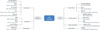 |
Figure 1. The mainstream PQC schemes and their standardization bodies |
1.1.1. NIST PQC standardization process
The transition to PQC by the NIST was formally initiated in 2016. The competition was structured through multiple rounds of public cryptanalysis, starting with an initial field of 82 submissions [20]. This extensive evaluation was conducted in July 2022 [13], when NIST announced the first four algorithms selected for standardization. The chosen set included one Key Encapsulation Mechanism (KEM), CRYSTALS-Kyber [14], designated as the primary replacement for classical key exchange; and three Digital Signature (DS) algorithms: lattice-based CRYSTALS-Dilithium [15] and FALCON [21], and stateless hash-based Sphincs+ [17]. By August 2024, NIST released the first three finalized Federal Information Processing Standards (FIPS 203 [22], FIPS 204 [23], and FIPS 205 [24]). In the finalized standards, NIST assigned generic and standardized names to the algorithms: CRYSTALS-Kyber became ML-KEM, CRYSTALS-Dilithium became ML-DSA, and Sphincs+ was renamed StateLess Hash-based Digital Signature Algorithm Standard (SLH-DSA).
In March 2025, the code-based Hamming Quasi-Cyclic (HQC) algorithm [25] was released as the fifth primary PQC algorithm, designated as a backup KEM to the lattice-based ML-KEM. In the meantime, NIST also initiated an additional competition for digital signature schemes; this process pushed 15 candidates to advance to the second round in October 2024.
1.1.2. PQC standardization process by other institutions (ISO, IEC, Kpqc)
Multiple global organizations beyond NIST are driving PQC standardization processes and deployment initiatives. The International Organization for Standardization (ISO) and the International Electrotechnical Commission (IEC), operating through Joint Technical Committee 1 (JTC 1), are crucial to aligning PQC with existing global security frameworks. This includes actively updating core standards, such as ISO/IEC 14888 [26] for digital signatures and ISO/IEC 18033 for encryption schemes, to incorporate NIST-recommended quantum-safe algorithms. Furthermore, ISO has independently standardized stateful hash-based signature schemes, notably XMSS [27] and LMS [28], by 2020. In addition, Classic McEliece [29] and FrodoKEM [30] schemes are also selected to be standardized. A distinct and strategic national effort is conducted in Republic of Korea, where the Republic of Korea post-quantum cryptography (KpqC) project was launched in 2021 to develop, evaluate, and standardize domestic PQC algorithms, including HAETAE (ML-DSA like), AIMer (Picnic like), SMAUG-T (ML-KEM like) and NTRU+ (NTRU like).
1.2. Necessity and scope of PQC hardware
The emergence of PQC is a direct consequence of a fundamental shift in the cybersecurity landscape, but its practical implementation is far from trivial. Although PQC algorithms, such as those based on lattices, resist the theoretical threat of quantum computers, their mathematical and algorithmic complexity imposes a significant overhead not encountered in classical RSA or ECC. This overhead manifests itself as larger key and ciphertext sizes and higher computational demands. The key size comparisons [31] are shown in Figure 2. For devices with strict limits on memory, power, and processing capacity, such as those in the Internet of Things (IoT), automotive systems, and smart cards, specialized hardware solutions are not simply an option, but a strategic necessity to ensure long-term security [18]. This imperative drives a market projected to surge in the future, reinforcing PQC hardware’s critical position in the global cryptographic migration.
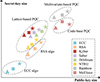 |
Figure 2. Key size comparisons between traditional and PQC schemes [31], triangles represent security level 1, squares represent security level 3, and pentagrams represent security level 5 |
The initial research scope in PQC hardware development is centered on exploring diverse implementation platforms to optimally balance efficiency and flexibility. (1) Mapping of standard PQC algorithms directly into general processors (e.g., Reduced Instruction Set Computing-V, RISC-V) or designing dedicated Instruction Set Extensions (ISEs) [32–35], offering high flexibility and portability for specific algorithmic deployment; (2) Mapping of the PQC algorithms on the Field-Programmable Gate Array (FPGA) [36–42], which is utilized for rapid prototyping and adaptable deployment, allowing designers to adjust to evolving standards; and (3) Application-Specific Integrated Circuits (ASICs) [43–49], the ultimate goal of achieving peak performance and ultralow power consumption necessary for large-scale mass-market deployment. To mitigate the inherent inflexibility of traditional ASICs, the dominant hardware design methodology has transitioned to DSAs [31, 50, 51] or Software-Defined Chips (SDC), which aim to deliver custom PQC acceleration with enhanced architectural flexibility. This approach is realized through hardware-algorithm co-design, which utilizes reconfigurable processing array and unified arithmetic units to achieve ASIC-like performance while ensuring the vital crypto-agility required to support evolving standards.
In addition, the scope of PQC hardware research extends critically into implementation security, addressing the fact that quantum-resistant mathematics does not inherently protect the physical chip. This direction focuses on identifying and mitigating classical, non-invasive threats that can compromise secret keys. Research is primarily categorized into two areas: Side-Channel Attacks (SCA) [52–55], which exploit physical leakages such as timing variations or power consumption during cryptographic execution (e.g., Differential Power Attack, DPA); and Fault Injection Attacks (FIA), where environmental stress (voltage, clock, or laser glitches) is used to induce errors and reveal secret information. To counter these pervasive threats, research is dedicated to developing robust hardware countermeasures, including advanced masking techniques, designed for constant-time operation.
1.3. Organization of the review
This review provides a comprehensive analysis of the current state of PQC chip design, addressing the critical transition from theoretical concepts to practical, robust hardware implementations. Section 2 offers an extensive overview and taxonomy of the main PQC algorithms categorized by their underlying mathematical hard problems, including lattice-based, code-based and hash-based schemes. The subsequent sections focus on the core engineering work: Section 3 dissects the functional hardware design challenges and computational bottlenecks inherent to each algorithmic family, specifically analyzing the implementation complexity of primitives like the Number Theoretic Transform (NTT) (lattice schemes) and parallel hash accelerators. Building on these requirements, Section 4 evaluates the practical implementation environment, examining various hardware platforms and design paradigms, from general-purpose processors and ISE to dedicated ASIC, FPGA, and the strategic adoption of agile PQC DSA. Section 5 analyzes the potential crypto-attack and hardware countermeasures, including the agile PQC DSA that supports multiple PQC families. Section 6 provides some insights and suggestions for future PQC hardware, including PQC DSAs and SCA/FIA resistant PQC hardware design. Finally, Section 7 provides forward-looking insights and perspectives on future PQC hardware, focusing on the need for agile, migratable, and resistant architectures, before the review is summarized in the Conclusion.
2. Overview of mainstream PQC algorithms
The development of PQC algorithms is a testament to the diversity of mathematical fields that can be used to create quantum-resistant primitives. Unlike the current public-key cryptography (e.g., RSA and ECC), which relies on a few well-understood number-theoretic problems that are susceptible to Shor’s algorithm, PQC explores a broad range of mathematical structures conjectured to be intractable for both classical and quantum computing systems. The mainstream PQC landscape is typically classified into five primary families based on their underlying hard mathematical problems: lattice-based, code-based, hash-based (symmetric-based), multivariate-based, and isogeny-based. Each of these families offers a distinct set of security assumptions, computational trade-offs, and hardware implementation challenges.
This section briefly introduces the basic hardness problem in each type of PQC, helping to provide a comprehensive understanding of the underlying principles that are essential for effective PQC chip design.
2.1. Lattice-based PQC (Kyber, Dilithium, Falcon, FrodoKEM)
Lattice-based cryptography is universally recognized as the most mature and promising family of PQC algorithms, with three of its schemes selected as primary NIST standards (Kyber [14], Dilithium [15], Falcon [21]). Its security is rooted in the computational difficulty in solving certain problems within high-dimensional lattices, which are discrete sets of vectors.
The foundational challenge is the SVP [10], which involves finding the shortest non-zero vector within a given lattice. However, the security of modern lattice-based schemes is typically derived from the LWE problem or the closely related Short Integer Solution (SIS) problem. LWE and SIS are particularly attractive because their average-case hardness has been rigorously proven to reduce to the worst-case hardness of classical lattice problems, providing a strong guaranty of security against quantum adversaries.
Standard LWE operations can be computationally intensive, prompting the exploration of structured variants to boost performance and reduce key sizes for practical implementation. The Ring-LWE problem [12] introduces algebraic structures, such as polynomial rings, to streamline complex matrix-vector operations via cyclic convolutions. This structural simplification allows for acceleration through techniques such as the NTT, resulting in significantly faster and more compact schemes. Further evolution led to Module-LWE [11], which operates on modules rather than rings, providing an optimal balance of performance, key size, and security against dedicated lattice attacks. The related Module-Learning With Rounding (Module-LWR) problem [8, 56, 57] replaces the error sampling found in LWE with deterministic rounding operations, simplifying arithmetic and potentially benefiting hardware implementation by requiring less true randomness. The module-LWE-based ML-KEM and ML-DSA schemes are illustrated in Figure 3.
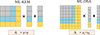
ML-KEM is based on the hardness of the MLWE problem, where a public matrix A is combined with a secret vector s and an error vector e to form the pseudo-random value b = As + e, ensuring secure key encapsulation. In ML-DSA, the signer’s secret consists of short vectors (s1, s2), and security relies on finding short solutions to the Module-SIS equation [A|I]×[s1; s2]=0, where A is a public matrix and I is the identity matrix. The core computational operation in ML-KEM is thus the modular matrix-vector multiplication (A × s) with small noise e, mimicking an approximate linear system to guarantee ciphertext indistinguishability. In contrast, ML-DSA’s signing process involves generating a response vector that must satisfy a shortness constraint relative to s1 and s2, followed by rejection sampling to avoid leaking the secret lattice basis. While both are module-lattice based, ML-KEM emphasizes the search/decisional-MLWE problem with (A, As + e), whereas ML-DSA additionally requires the signer to construct a short vector solution in the Module-SIS problem, linking authenticity to the infeasibility of short vector discovery.
(1) CRYSTALS-Kyber (ML-KEM [22]): Selected by NIST as the primary KEM for key exchange and encryption. Kyber is based on the Module-LWE problem. It was chosen for its strong security proof, excellent performance in encapsulation and decapsulation, and relatively small key sizes, making it suitable for a wide range of applications, from cloud servers to resource-constrained IoT devices. Hardware implementations of Kyber heavily rely on accelerating polynomial multiplication using the NTT.
(2) CRYSTALS-Dilithium (ML-DSA [23]): Selected by NIST as the primary digital signature algorithm. Dilithium is based on a module-lattice version of the SIS problem and employs the “Fiat-Shamir with Aborts” paradigm, utilizing rejection sampling to ensure the signature distribution is independent of the secret key. Its design prioritizes strong security and robust performance in key generation, signing, and verification operations. Optimized hardware designs often feature unified architectures capable of performing both Kyber and Dilithium’s polynomial arithmetic.
(3) FALCON [21] (Fast Fourier Transform over the NTRU-lattice-based Digital Signature Algorithm, FN-DSA): A second lattice-based signature scheme selected by NIST for standardization [21]. Falcon’s security is based on the SIS problem over NTRU lattices. It is distinguished by generating the smallest signature sizes among the NIST finalists, making it ideal for applications sensitive to bandwidth or storage limitations. Unlike Kyber and Dilithium, FALCON uses a complex Gaussian sampling routine and relies on the Fast Fourier Transform (FFT) for fast polynomial multiplication, which introduces unique hardware design challenges.
(4) FrodoKEM [30]: This KEM scheme is based on plain LWE without any algebraic structure (i.e., not Ring-LWE or Module-LWE), using standard integer matrices. FrodoKEM advanced to round 3 of the NIST process and was not selected as the final drafts. However, Falcon was selected by ISO as the final standard. Although it offers highly conservative security assumptions, its lack of algebraic structure prevents the use of efficient NTT acceleration, resulting in comparatively larger public keys and lower performance. This computational overhead ultimately led to its discontinuation in the standardization process due to low deployment interest, although it remains a crucial academic reference for pure LWE security.
2.2. Code-based PQC (HQC, Classic McEliece, BIKE)
Code-based cryptography is one of the oldest and most thoroughly studied branches of PQC, originating with the work by McEliece in 1978 [58]. The security of this family is founded on the difficulty of decoding a general linear error-correcting code, an NP-hard problem. An attacker attempts to recover the original message by decoding a ciphertext that has been deliberately corrupted by a small error vector; however, without the secret knowledge of the code’s structure, this task is computationally infeasible.
(1) HQC: HQC is a modern KEM scheme based on quasi-cyclic codes [25], specifically combining concatenated Reed-Muller (RM) and Reed-Solomon (RS) codes. HQC was recently selected by NIST as the fifth standardized asymmetric algorithm, serving specifically as a backup KEM to the lattice-based ML-KEM. The brief illustration of the HQC scheme is shown in Figure 4. Its inclusion ensures cryptographic diversity, relying on completely different mathematical assumptions than the dominant lattice family, thereby mitigating the risk of a systemic failure should a weakness be found in lattice assumptions. HQC, like other code-based schemes, exhibits strong security, but introduces challenges in hardware implementation related to its large memory footprint and the complexity of the syndrome decoding process.
(2) Classic McEliece: The seminal code-based encryption scheme [29], Classic McEliece, uses algebraic Goppa codes to construct a trapdoor mechanism. The strength of McEliece lies in its long-term security confidence, having resisted decades of cryptanalytic attempts. However, its primary practical drawback is the necessity for very large public keys, typically on the order of several megabytes. This key size penalty severely limits its deployment feasibility and requires efficient memory organization, leading NIST to acknowledge it as a robust scheme (without standardization), but standardized finally by ISO.
(3) BIKE: The BIKE scheme [59], a prominent KEM in the NIST PQC process, is a modern code-based algorithm whose security is rooted in the computational hardness of decoding quasi-cyclic error-correcting codes. The strength of BIKE lies in its distinct mathematical foundation, providing crucial cryptographic diversity and a strong alternative to the lattice-based standards. However, its primary practical drawback is the substantial computational overhead and high latency incurred during the decapsulation process, particularly on resource-constrained hardware. Benchmarks on embedded platforms show that BIKE’s Level 5 key generation can last over multiple milliseconds, representing a significant slowdown compared to lattice schemes. This increased computational cost, coupled with higher performance variability (4–5% standard deviation) due to its probabilistic decoding process, severely limits its deployment feasibility in time-sensitive or high-frequency environments. Consequently, achieving acceptable performance requires extensive hardware-software co-design efforts focused on optimizing the decoding algorithm’s performance, despite BIKE achieving exceptionally low memory usage.
2.3. Hash-based PQC (Sphincs+, XMSS, LMS)
Hash-based cryptography provides a simple and exceptionally reliable method for digital signatures, deriving its security from the one-way and collision-resistant properties of cryptographic hash functions (such as SHA-2 or SHAKE-256). Since no efficient quantum algorithm is known to invert a general hash function, these schemes are inherently quantum-resistant. The primary trade-off is often the computational intensity and complexity of managing private-key usage.
(1) Stateful Hash-Based Signatures (XMSS, LMS): The root of this family lies in One-Time Signature (OTS) schemes (such as Lamport signatures), where a key pair must be used to sign only a single message. To achieve many-time signatures, the Merkle Signature Scheme (MSS) [60] uses a hash tree (Merkle Tree, MT) where the leaves are the hash values of the individual OTS public keys. The root of the tree serves as the single public key for the scheme. XMSS [27]: XMSS and its multitree variant XMSS MT provide robust forward-secure signature schemes that require the signer to track the state, which leaf key was last used-to prevent key reuse. XMSS has been standardized by ISO/IEC and published as Request For Comments (RFC) 8391 by the Internet Engineering Task Force (IETF) [61]. LMS [28] is another popular Merkle-tree-based state signature scheme. Stateful schemes are highly secure, but their reliance on secure state management introduces deployment risks if the state is lost or corrupted.
(2) Stateless Hash-Based Signatures (Sphincs+/SLH-DSA): Sphincs+ (SLH-DSA): The Sphincs+ hash-based stateless signature scheme [17] was developed to eliminate the burdensome state management required by XMSS and LMS. It achieves statelessness through the complex integration of three components: the Winternitz OTS variant (WOTS+), the Forest of Randomized Trees (FORS) and a Hypertree structure, which is shown in Figure 5. Sphincs+ provides security diversity by relying on symmetric primitives, and it was selected for standardization by NIST as SLH-DSA (FIPS 205), intended as a non-lattice-based backup signature scheme. The scheme is computationally intensive, making its hardware acceleration (particularly the underlying SHAKE-256 or SHA-256 operations) a crucial research topic.
The Multi-Party Computation in the Head (MPCitH) paradigm [62] also belongs to a symmetric-based scheme, which leverages techniques derived from symmetric cryptography to construct efficient Zero-Knowledge Proofs (ZKP), which are then used to build digital signature schemes. The basic principle involves a prover simulating a three-party computation of a secret function “in their head” and demonstrating knowledge of the private key without revealing it.
(3) Syndrome-Decoding-in the-Head (SDitH): A signature candidate in the NIST’s additional signature competition that employs the MPCitH construction. SDitH’s security is based on conservative code-based assumptions (traditional decoding problems), offering a unique blend of code-based security and ZKP efficiency. This represents a PQC scheme design of a code-based signature based on traditional decoding problems of an MPCitH construction, after Picnic.
2.4. Multivariate-based PQC (UOV, Rainbow)
Multivariate cryptography relies on the difficulty of solving large systems of simultaneous multivariate polynomial equations (typically quadratic) over a finite field. This problem is known to be NP-hard, giving it quantum resistance.
While several early multivariate encryption schemes were cryptanalyzed by classical computers, the family remains relevant for digital signatures. The Rainbow signature scheme [63, 64] (based on the construction of unbalanced oil and vinegar [65]) was a finalist in the NIST competition, although it was later withdrawn due to a successful classical attack on its parameters. UOV also remains in the NIST additional DS standardization process. Multivariate signature schemes are known for their high speed and potentially small signature sizes but require efficient hardware processing of large dense matrices.
The signature generation process is illustrated in Figure 6, which involves Gaussian elimination and quadratic matrix vector multiplication, which is the critical computational bottleneck during signing and verification.
2.5. Isogeny-based PQC (SIKE, SQIsign)
Isogeny-based cryptography constructs its security from the difficulty of finding a path between two super-singular elliptic curves linked by an isogeny map [66]. This approach is distinctive in offering the smallest key sizes among all major PQC families, which was its primary advantage during the NIST competition.
SIKE [67–69] was an alternate candidate in the NIST KEM category. However, a major setback occurred in 2023 [70] when a classical computer attack was found that could compromise the scheme in about an hour. While SIKE was withdrawn, the family is still being researched, with new constructions such as SQIsign and cSIDH aiming to build robust signatures and KEMs from the isogeny problem.
Isogeny-based PQC is rooted in long-integer modular arithmetic over large prime fields, departing entirely from the polynomial-ring arithmetic of lattice schemes. The primary computational bottleneck is centered on the efficient execution of multi-precision arithmetic, specifically modular multiplication and reduction on integers often exceeding 768 bits [71]. Furthermore, the high-level cryptographic operation of isogeny graph traversal, the means by which the shared secret is established–involves repeated curve arithmetic (point addition and doubling), demanding meticulous scheduling of these long-integer operations.
3. PQC hardware design challenges and bottlenecks
The transition from theoretical PQC algorithms to a practical, secure, and efficient hardware implementation represents a complex engineering challenge. While the mathematical security of these algorithms is paramount, their physical realization in silicon introduces a new set of design and optimization, which is crucial for PQC research and deployment. Unlike traditional public-key cryptosystems (RSA [3], ECC [4]), which rely primarily on modular multiplication of large integers, PQC schemes involve computationally intensive high-degree polynomial arithmetic, dense matrix operations, and complex control flows. This complexity necessitates a fundamental rethink of traditional hardware design paradigms.
The major challenges in PQC hardware can be summarized in these critical aspects.
- (1)
High Computational Complexity and Diverse Calculation Patterns. Unlike the uniform mathematical operations of ECC and RSA, PQC schemes leverage fundamentally distinct mathematical structures. This results in a wide array of specialized and high-cost computational primitives that are entirely dependent on their mathematical problems. For example, lattice schemes require complex polynomial arithmetic acceleration via the NTT process. Code-based schemes are restricted by complex syndrome decoding algorithms. This algorithmic diversity demands specialized processing modules, which also requires software-hardware co-design. Efficient algorithms, such as NTT [72] and Karatsuba [73], can efficiently reduce the complexity of the calculations and accelerate these schemes. The efficient mapping of these algorithms on the hardware affects the overall performance of the PQC hardware.
- (2)
High Storage Pressure. Compared to classical Public Key Cryptography (PKC), PQC schemes involve significantly larger cryptographic material, including public keys, private keys, and ciphertexts or signatures, which is shown in Figure 2. For example, Classic McEliece requires public keys on the order of several megabytes [29, 58], placing immense pressure on the device memory and communication bandwidth. Even highly optimized lattice schemes can increase the Transport-Layer Security (TLS) 1.3 handshake size by up to several times compared to classical approaches [74–77]. This substantial data footprint requires hardware designers to devise highly efficient on-chip memory organization schemes and intelligent scheduling to balance the memory access and the latency of calculations.
- (3)
Flexible Control and Scheduling Challenge. The multi-phase and often non-deterministic nature of PQC algorithms mandates a complex control unit. This challenge manifests itself in two ways: (1) Secure Scheduling: Algorithms such as Dilithium and Kyber use rejection sampling, where hardware must employ rigid control logic to enforce constant-time execution [78, 79] and prevent timing leakage related to secret key or random number generation. (2) Algorithmic Agility: As PQC standards continue to evolve (e.g., the NIST additional signatures process) [13], the hardware must be equipped with flexible scheduling and data path capabilities (often achieved via DSAs) to seamlessly support multiple algorithmic families (e.g., lattice and code) and rapidly adapt to new standards, ensuring that the system is future-proof. Successful management of this dilemma among high complexity, high storage, and flexible and secure control is paramount to a successful PQC chip design effort.
3.1. Lattice-based schemes: NTT and polynomial arithmetic
Lattice-based cryptography forms the backbone of the PQC transition due to its strong security proofs and performance balance. The primary computational bottleneck in these structured lattice schemes (e.g., Ring-LWE, Module-LWE) is the polynomial multiplication required for key generation, encapsulation, and decapsulation. According to the parameters of the polynomial and modulus value, mainstream polynomial multiplications can be divided into two types:
- (1)
NTT-based polynomial multiplication (Kyber, Dilithium, Aigis). A modification of the FFT suitable for prime-coefficient fields, the NTT algorithm successfully reduces the computational cost of multiplication to 𝒪(nlogn).
The application method for multiplying n-degree polynomials is contingent upon the chosen modulus:
- (a)
When the modulus polynomial is xn − 1, a direct n-point NTT is immediately applicable;
- (b)
Conversely, if the modulus polynomial is xn + 1, the result can be obtained either by performing a 2n-point NTT followed by a final modulus operation, or by using the Negative Wrapped Convolution (NWC) technique, which is discussed later in this work [80], utilizing an n-point NTT for the computation.
In the mainstream quantum-resistant cryptographic algorithms, such as Kyber or Dilithium, the polynomial ring modulus is typically mandated to be xn + 1. The NWC technique is the preferred method for efficiently calculating the product C = A × B in the polynomial ring ℤq[X]/(xn + 1). A key feature of this approach is its use of n-order NTT and Inverse NTT (INTT) without necessitating an explicit reduction step. For the NWC approach to be viable, the modulus q must satisfy the condition
 . This ensures the existence of a 2N-th primitive root γ2N within the prime coefficient field GF(q). This methodology, however, necessitates preparatory calculations before the NTT and subsequent calculations after the INTT. Denoting the scaled coefficients as
  ,
,  , and
, and  , the convolution of A × B over the ring ℤq[X]/(xn + 1) is expressed as
 ![Mathematical equation: $$ \bar{c} = \text{ INTT}_n [\text{ NTT}_n(\bar{a}) \text{ NTT}_n(\bar{b})]. $$](/articles/sands/full_html/2026/01/sands20250037/sands20250037-eq5.gif)
In essence, the n-point NTT is applied to the pre-scaled vectors
 and
and  . The resultant scaled vector
  then yields the desired convolution result c after post-scaling. The NWC method effectively avoids the need for 2n-point NTT/INTT operations, thereby eliminating the explicit reduction stage. While this introduces an additional overhead from the NTT preprocessing and post-INTT processing, these costs can often be fused with the main NTT/INTT operations in optimized implementations. Consequently, the time penalty associated with these extra steps becomes negligible in both software and hardware execution environments, an aspect that will be further detailed in the remainder of this section.
 - (a)
- (2)
Schoolbook, Karatsuba, Toom-Cook: NTT-unfriendly polynomial multiplications (Saber, LAC, NTRU). In many PQC schemes, the polynomial parameters are incompatible with NTT-based multiplication because the polynomial length and the modulus values fail to satisfy the necessary congruences, specifically
 or
or  .
.Consequently, other high-performance multiplication algorithms, such as Karatsuba or Toom-Cook, are instead employed to decrease multiplication complexity and accelerate the cryptographic schemes. The Karatsuba algorithm, recognized as the first highly efficient multiplication method [81], achieved a reduction in computational complexity from 𝒪(n2) to 𝒪(nlog23)≈𝒪(n1.585). This innovative approach utilizes a recursive method where the computation is split into two halves, conventionally requiring four sub-multiplications, which are cleverly optimized to require only three.
Large numbers or polynomials A and B are separated into two halves according to the following definitions:
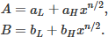 (1)
(1)
These decomposition formulas divide the input into lower (L) and higher (H) components. If A and B are n-degree polynomials, the factor x in the formulas represents the weight of 2n/2 that would be used for n-bit large integers.
The direct multiplication of A and B is initially expressed as

To apply the Karatsuba complexity reduction, the central cross-product term is reformulated, allowing the entire multiplication to be calculated with three products instead of four:
![Mathematical equation: $$ a_H b_H x^n + \left[(a_L+a_H )(b_L+b_H ) - (a_H b_H+a_L b_L )\right]x^{n/2} + a_L b_L. $$](/articles/sands/full_html/2026/01/sands20250037/sands20250037-eq13.gif)
This reformulation decreases the number of multiplications from four to three per iteration, though the total number of additions increases from two to six. When the Karatsuba algorithm is applied recursively, the quantity of multiplications scales down proportionally. With every step of recursion, the computational complexity for the multiplication effectively decreases to 75% of the original four-product method.
In hardware realizations of Karatsuba [82], multi-dimensional variations exist to achieve further minimization of the multiplication complexity. Specifically, in the hardware implementation of the multi-dimensional Karatsuba algorithm, a significant challenge remains in minimizing the storage requirements (registers) and the number of additions during the pre-addition and post-addition phases.
3.1.1. Review of NTT hardware
The efficient design of NTT hardware is probably the hottest research topic in PQC hardware design. To implement an efficient NTT module on PQC hardware, at least the following three challenges need to be addressed.
- (1)
Overheads of Pre/Post-processing (Additional Multiplications and shuffling in NWC). To mitigate the additional pre/post processing that occurred by NWC methods, the work [83] first merges the preprocessing into the normal data flow and reduces the multiplication complexity on an embedded general processor, which avoids the additional cycle overheads of preprocessing. The idea is then extended to the work [84], which is a FPGA-based NTT accelerator. In that work, post-processing (including additional post-multiplication in NWC and n−1) is avoided by further merging these operations with the normal NTT data flow. However, the structure in ref. [84] still needs an additional shuffling process before the NTT and after INTT processes. In addition, the Montgomery factors introduced if Montgomery reduction is used in the work [84]. The above ideas are extended in the work [31, 85] and additional processing does not incur additional time overhead.
Based on the research context mentioned above, we use the work [31] as an example to illustrate how additional overheads are avoided.
The NWC-NTT is formally defined as
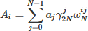 , while the Inverse NWC-NTT (NWC-INTT) is given by
 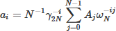 , where ωN and γ2N represent the n-order and 2n-order primitive roots of unity, respectively, satisfying the conditions γ2n = ωn = 1.
Building upon prior research [39, 83, 84], the powers of γ (the scaling factors) can be mathematically incorporated into the calculation of both the NTT and INTT transformations. This leads to the following recursive split equations for the NTT:
 (2)
(2)
The structure of this computation, with addition occurring after multiplication, is characteristic of the Cooley-Tukey (CT) butterfly design pattern.
A similar derivation yields the recursive split equations for the INTT, shown below:
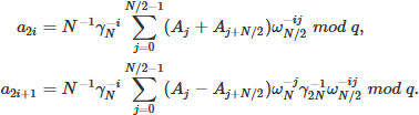 (3)
(3)
This feature demonstrates the feasibility of reusing twiddle factors, provided the second term in eq. (3) is modified as follows:
 (4)
(4)
The operational data flow and the methodology for twiddle factor reutilization for an 8-point NTT and INTT are visually represented in Figure 7.
Consequently, based on the findings in works such as refs. [31, 83, 84], modern NTT hardware implementations [86–88] can be designed without needing to allocate resources for the perceived “additional overheads” of NTT/INTT preprocessing and post-processing.
- (2)
Design choice of data-flow architecture. Like the FFT hardware design, most of the NTT hardware almost obey two ways, which is shown in Figure 8:
- (a)
Vectorized method to calculate multiple butterfly operations in the same layer each time [31, 50, 85, 89, 90];
- (b)
Radix-2 Multi-path Delay Commutator (R2MDC) method to execute multi-layer butterfly operations in pipeline [91].
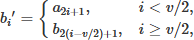
In the previous vectorized NTT hardware design, the works [89] implemented a constant-geometry ping-pong single-port calculation framework. It focused on the embedded platform and executed one modular multiplication per cycle. The work [90] adopted a vectorized in-place ping-pong execution method to improve the parallelism. In that work, there are at least 12 permutation networks adopted to process the coefficient permutations among the input/output vectors, which incurs significant overhead for multiplexers and interconnection. Moreover, the number of permutation networks depended on the vector parallelism. In the later work [50], the permutation networks are reduced to only 4 permutation networks through the dedicated permutation patterns, and the amount of permutation networks is independent of the parallelism, which is shown in Figure 9. The basic idea to save the permutation networks is to map the logical addresses to the physical address. The mapping relation will change when data pass through the NTT output networks and INTT input networks, such as
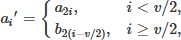 (5)
(5)
 (6)
(6)
Therefore, the utilization rate of permutation networks is increased and the number of permutation networks is reduced. And the correctness of the network topology has been proved in the later work [92]. The NTT design in ref. [91] adopted an optimized pipelined NTT structure inspired by the R2MDC FFT structure introduced, which avoid a large number of complex memory accesses. The R2MDC FFT architecture requires fewer and simpler memory accesses compared to the vectorized method. And it is also better at processing multiple NTT/FFTs continuously. For a 256-point R2MDC FFT/NTT, it only needs two input coefficients per cycle to achieve a 100% utilization rate of the butterfly units. The details of R2MDC circuit are shown in Figure 10. This architecture can process both radix-2 decimation-in-time FFT/NTTs and radix-2 decimation-in-frequency FFT/NTTs by using different butterfly units and twiddle factors. In addition, it can process both the FFT and the Inverse FFT (IFFT), with the difference being that the IFFT requires additional postprocessing and different twiddle factors. This architecture also needs additional pipeline loading latency to pre-fill the pipeline, and it also needs lots of registers or Static Random Access Memory (SRAMs) to buffer the coefficients in each stage.
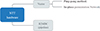
Figure 8. Two different ways to implement NTT hardware
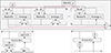
Figure 10. The typical architecture of R2MDC NTT [91]
Therefore, the features of these two major ways of implementing NTT are summarized in Table 1. Designers can choose the appropriate NTT architecture based on the features listed in Table 1.
- (a)
- (3)
Efficient and Reusable Butterfly Unit design. Once the whole architecture of NTT is fixed, the scheme of butterfly unit also needs to be determined. One of the important parts of the butterfly unit is the design of the reduction methods and the module design, which need to balance the reduction efficiency and flexibility supporting different modulus. The mainstream reduction methods can be divided into the following methods.
- (a)
Dedicated shift-and-subtraction reduction [84, 86, 91]. This method applies to dedicated hardware for a specific algorithm. For instance, the modulo operation with modulus value 12289 can be adjusted into a sequence of shifting and subtractions. Due to the equation
 , then z = 214z[27 : 14]+z[13 : 0]=212(z[27 : 26]+z[25 : 24]+z[23 : 22]+z[21 : 20]+z[19 : 18]+z[17 : 16]+z[15 : 14]) − (z[27 : 26]+z[27 : 24]+z[27 : 22]+z[27 : 20]+z[27 : 18]+z[27 : 16]+z[27 : 14]) + z[13 : 0] [91]. Therefore, the costly modular operations can be reduced to only the shift and subtraction bit operations. Other hardware implementations [86] followed this method to simplify modular operations, which only adapt to one modulus value and struggle to support multiple primes.
 - (b)
Look-up table-based reduction [89, 93]. In aim to support multiple-values’ modulus operations, the chip [89] instantiates all common primes and utilizes the LUTs to achieve some flexibility. These methods can simplify the reduction module to some degree, which is hard to support in any prime.
- (c)
Complete Montgomery-based reduction [31, 50]. To adapt to any primes within some bit size, optimized Montgomery reduction is utilized in ref. [31] and the work followed by ref. [50].
The block diagram of each reconfigurable Arithmetic Element (AE) is shown as Figure 11. The AE module depicts the combination of GS-Butterfly Function Unit (GS-BFU) and CT-Butterfly Function Unit (CT-BFU) with optimized Montgomery modular multiplication hardware construct the framework of AE. Montgomery reduction method is used to achieve modular operation. This is because only Montgomery method is adaptable to the reduction in binary field. Hybrid reduction including both integer reduction and binary reduction are achieved. The detailed process is illustrated in Algorithm 1. The correctness of Montgomery method in GF(2n) is easy to prove: r = ⟨r⟩p = ⟨t × R−1⟩p. And due to r = (t + s1 × q)/R, the degree of r is not greater than 2n − n = n.
The Montgomery reduction method is also optimized through reducing the addition process to half width in step 3, which reduces the resource usage, which is shown in Algorithm 1. Besides, the AE module also incorporates the low-power design, and the readers can refer to ref. [31] for details.
In addition to modulus difficulty, factor scaling is also a problem in considering butterfly unit design. Figure 12 shows the hiding strategy in ref. [31]. In LWE-type cryptographic schemes, the scaling factor N−1 and the Montgomery factor introduced during the As computation are effectively masked using two distinct modes of the AE configuration.
The initial technique conceals these factors by setting the AE to its Multiplication-Addition (Mul-Add) mode. This scaling is applied during the addition step of As + e, which occurs immediately after the INTT transformation. The alternative approach involves configuring the AE in Addition-Multiplication (Add-Mul) mode. This mode applies the scaling during the final summation process of As, which is performed before the INTT. Crucially, neither of these two methods introduces any extra overhead concerning hardware area or clock cycles.
While leveraging the reconfigurable Arithmetic Logic Unit (ALU) successfully prevents time overhead, it incurs increased power consumption due to the greater number of multiplication operations executed.
Conversely, other notable hardware implementations [43, 44, 84] propose a technique where a fractional modulus of 1/2 is applied within each butterfly operation. This method achieves the required 1/n scaling throughout the entire INTT process. Furthermore, to eliminate the need for Montgomery factors, these designs often employ either the native modular reduction method or the Barret reduction technique.
- (a)
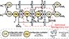 |
Figure 11. The scheme of reconfigurable AE [31] |
Comparisons with the two major NTT architectures
Input: a, b, q: integers in Zq or polynomials in GF(2n); R: n-bit Montgomery factor
Pre-computation: u = s/q mod R; where s = −1 in Zq, s = 1 in GF(2n)
Output: r = a b R−1 mod q
step 0: t = a b; [tH, tL] ← t; where ← means dividing into two halves
step 1: s1 = tL u mod R
step 2: s2 = s1 q; [s2H, s2L] ← s2
step 3: r = tH + s2H + flag (tL! = 0); where flag=1 in Zq, flag=0 in GF(2n)
step 4: r = r − q (r ≥ q); where ≥ denotes not less than on values in Zq and degrees of polynomial in GF(2n)
//For GF(2n), all + and − operations denote xor operations
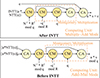 |
Figure 12. Scaling hiding strategy in ref. [31] |
3.1.2. Review of Karatsuba/Toom-Cook hardware
As discussed above, the Karatsuba algorithm [73, 81] has become the most widely used high-efficiency method for polynomial multiplication acceleration when the modulus of polynomial coefficients does not meet the requirements of the efficient NTT algorithm. To accelerate polynomial multiplication [36, 94–97], Karatsuba or Toom-Cook is used on Saber and NTRU PQC hardware.
When comparing Karatsuba and Toom-Cook hardware, Karatsuba hardware is equipped with a simple architecture, which can be stacked with multiple dimensions recursively. Although lower complexity is adopted in the Toom-Cook algorithm [96], diverse dimensions are difficult to stack in hardware implementation due to complex evaluation and division operations. The state-of-the-art Toom-Cook hardware uses a 1-layer 4-term Toom-Cook [96], which saves a number of 9/16 multiplications. The state-of-the-art Karatsuba hardware uses the 8-layer Karatsuba algorithm [94, 97], which saves up to 90% of multiplications. The comparison table between the Karatsuba and Toom-Cook hardware is depicted in Table 2.
Comparisons between Karatsuba and Toom-Cook hardware
Based on this design paradigm, the core challenge of Karatsuba hardware can be summarized as the following points:
- (1)
Maximize the utilization rate of multiplication hardware and parallelize between Pre-Add/Post-Add and multiplication;
- (2)
Reuse the adders and registers in the Pre-Add and Post-Add stages.
The hierarchical Karatsuba calculation framework has been adopted by several implementations, including those detailed in refs. [94, 97]. This framework is structured into two distinct layers: the kernel layer and the scheduling layer.
Specifically, the kernel hardware in the LWRpro design implements a recursive 4-level version of the Karatsuba algorithm [94]. This kernel layer, which is composed of 81 multipliers and associated adders, is engineered to process degree-16 polynomial multiplication in a single invocation. The scheduling layer’s primary role is to convert the overall computational task into a series of degree-16 polynomial multiplications, matching the capability of the kernel hardware via the Karatsuba decomposition method. The entire algorithm for this hierarchical Karatsuba framework is described in Algorithm 2.
Input: A, B: degree-256 polynomial
Output: Res = AB mod x256 + 1
for (i=1; i≤81; i++) do
▹ Pre-process:
(PreRegA, αi′) ← Preprocess (PreRegA, InAi)
(PreRegB, βi′) ← Preprocess (PreRegB, InBi)
▹ Kernel calculation:
(PH, PL) ← Kernel_degree16mul (αi′, βi′)
▹ Post-process:
(t7, t6,..., t0) ← Map2level (PH, PL)
if a degree-64 sub-polymul has done and j ≤ 7 then
j = 0
Res ← Res + Map2level_serial (tj)
j = j + 1
end if
end for
return Res
Input vectors containing 16 coefficients are transformed into the required Karatsuba input format by preprocessing circuits; simultaneously, the preprocessing registers are updated. The kernel hardware then processes Karatsuba input multiplication, and the resulting degree-64 sub-polynomial multiplication results are directed to 128-coefficient intermediate registers, denoted t, through one segment of the post-processing circuits.
On the preprocessing side of the scheduling layer, a compact input preprocessing technique was developed to minimize the required registers and adders. To maximize the reusability of data stored in the input registers, the sequence in which multiplications are executed is deliberately re-organized. This module converts the initial degree-64 polynomial input into nine degree-16 polynomials required for the Karatsuba method. The preprocessing steps for both polynomial operands are identical. Calculating a single degree-64 sub-polynomial multiplication requires nine clock cycles. Pre-processing register groups are utilized to temporarily cache certain inputs or outputs, supporting future addition operations needed to compute Karatsuba intermediate values. These registers eliminate extra idle (bubble) cycles that would otherwise be spent waiting to read the second operand values for addition, and they also store some intermediate results. The data retrieval order of the input memory is also restructured to ensure maximum data reusability. This optimization requires only one adder group and two register groups, each with a width of 16 coefficients (1-coefficient width). When compared against a fully-unrolled architecture, this approach saves four adder groups and three register groups, although it requires the inclusion of additional multiplexers.
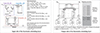 |
Figure 13. Input and output modules in the Karatsuba scheduling layer [94] |
On the post-processing side, a sequential hardware-efficient Karatsuba scheduling strategy was proposed to specifically mitigate the overhead associated with output scheduling. The principal objective of this strategy is to ensure that the result of every multiplication contributes immediately and fully to the final result without requiring additional registers. In the output scheduling process, the results of each multiplication are routed along different paths to directly influence the corresponding result registers. This design effectively eliminates the need for six 16 coefficient output register groups and two adder groups, each with a width of 16 coefficients (see Figure 13).
This foundational design concept has been adapted and extended in subsequent hardware implementations, such as that found in ref. [97], with only minor variations introduced on the input side. The utilization of multi-dimensional iteration, time-space parallelism, and a high degree of data reuse in this structure is expected to influence future Karatsuba hardware designs, which may achieve further reductions in the overhead associated with registers and adders.
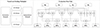 |
Figure 14. Efficient Toom-Cook hardware in ref. [96] |
For Toom-Cook hardware, the core challenges of Toom-Cook hardware are as follows:
- (1)
Maximize the utilization rate of multiplication hardware and parallelize between Pre-Add/Post-Add and multiplication;
- (2)
Avoid division operation and efficient scheduling of memory accesses.
In work [96], the design incorporates seven parallel point multipliers, which is shown in Figure 14. This parallel structure is inherently utilized by partitioning the Toom-Cook algorithm into three phases: Evaluation (Pre-Add), Multiplication, and Interpolation (Post-Add). The architecture features dedicated data paths for each phase, allowing the core multiplication stage to operate efficiently while the evaluation and interpolation logic manage the complex data flow, thus maximizing the utilization rate of the underlying multiplier hardware.
The high cost and latency associated with division operations, which are typically necessary during the interpolation (Post-Add) phase of Toom-Cook, are completely circumvented by implementing division as inverse multiplication. The required inverse numbers are pre-calculated and permanently stored in dedicated registers, effectively eliminating the overhead of division from the runtime critical path. Currently, to mitigate the large data footprint and sequential access limitations of classic PQC multiplication, the design adopts the tooth-shaped Toom-Cook multiplication, which splits the polynomial with a stride factor of 4, allowing the resulting polynomial to be ring-reduced on-the-fly. This stride technique significantly improves memory scheduling by facilitating stride memory access patterns.
Despite this, this work only achieved a 4-term Toom-Cook algorithm, and the efficient high-dimensional recursive Toom-Cook hardware design is still an open problem.
3.2. Code-based schemes: Large keys, syndrome implementation and inversion hardware
Unlike lattice-based PQC hardware, massive key storage, complex syndrome decoding, and problem inversion are involved in code-based PQC hardware [98–105].
3.2.1. Review of inversion hardware
In cryptographic algorithm computations, inverse operations within the algebraic structures of rings or fields are frequently involved. Three primary inverse calculation methods are employed: Fermat’s little theorem, Look-up table method, and the Extended Euclidean Algorithm (EEA). The comparison table is shown in Table 3.
- (1)
Fermat little theorem: The theoretical foundation of Fermat’s little theorem lies in the equation of
 for any group, where q represents the group’s order. Consequently, its inverse computation requires substantial additional operations, such as squaring and multiplication. This results in higher computational complexity, making it more suitable for software implementation as it allows efficient reuse of multiplication resources on general-purpose processors. The reference software implementation of Classical McEliece [29, 106, 107] and HQC [25] adopts this method.
 - (2)
Look-up table based inversion: This method calculates the inversion through storing all the inverses of any elements in some field, just like GF(2m). This method adapts to small-size finite-field while consuming large memory resources. The hardware implementation [38, 108] adopted this method to execute inversion on FPGAs, which have large memory resources. However, the inversion throughput is also limited due to the limitation of read ports of Block-RAMs (BRAMs). It is difficult to execute the parallel inversion.
- (3)
EEA: In contrast, the EEA primarily utilizes shift or eXclusive OR (XOR) operations, offering lower computational overhead that better meets throughput- critical requirements or latency-sensitive hardware implementations.
The classical EEA fundamentally operates as a division-by-rotation procedure, defined by the iterative calculation
 , where the remainder r is derived from the division a = bq + r. If the input large numbers or polynomials, a and b, are co-prime, the final value of b will be either 1 (for numbers) or a constant (for polynomials). However, the classical EEA is rarely used in practice due to its heavy reliance on division operations. Since the cost of division is prohibitive for direct mapping on both general-purpose processors and dedicated hardware accelerators, improved inversion algorithms are standard for implementation.
The Almost Inverse algorithm was proposed in 1999 [109] to address this limitation. It replaces division operations with more hardware-acceptable shifts and XOR operations. Each iteration involves generating a quotient coefficient t that translates into three possible exchange matrices. The appropriate matrix selection, and whether to perform a swap, shift, or negation, depends on the characteristics of the input data in each cycle. The overall effect of this approach is the transformation of division into swapping, shifting, and XOR operations, making it significantly more amicable to both software and hardware platforms. Despite its benefits, the Almost Inverse method is limited because its operational sequence–and thus its execution time–is dependent on the input data. This non-constant-time execution is unsuitable for cryptographic operations, which strictly require constant-time execution for sensitive data to prevent leakage via time side-channels. In response to this security concern, Hulsing introduced a constant-time implementation of the extended Euclidean inverse algorithm in 2017 [95]. This work achieves constant-time efficiency by exploiting built-in general-purpose processor instructions, such as conditional swap and XOR. Additionally, the maximum number of iterations is fixed by pre-estimating an upper bound. Building on this, Bernstein presented a low-complexity constant-time extended Euclidean algorithm in 2019 [110].
(a) Vectorized coefficient inversion hardware: The work [31] adopted vectorized-coefficient inversion with a reduced Euclidean inversion algorithm, which is shown in Figure 15. Up to about 25% And-XOR gates during polynomial inversion can be reduced in hardware implementation. This optimization is based on the conclusion that was always established before Mul-Add operation: max(deg(b),deg(c))iter = i ≤ max(deg(b),deg(c))iter = i − 1 + 1 and max(deg(b),deg(c))iter = i ≤ min(i, n), where the aim is to calculate degree-n
 , two helper polynomials, b and c, are utilized to record the matrix coefficients. Readers can refer to ref. [31] for detailed proof.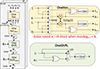
Figure 15. Vectorized-coefficient inversion hardware in ref. [31]
(b) Large-size inversion hardware: The state-of-the-art large-size inversion hardware is ref. [111], which is based on the algorithms [110, 112]. Readers can refer to refs. [111, 112] for further details of inversion hardware or algorithms.
The comparisons among three different inversion methods
3.2.2. Review of efficient memory scheduling
The key size of code-based PQC schemes, especially for Classic McEliece, can reach several megabytes, placing immense pressure on device memory, making pure software deployment difficult in constrained environments, as well as for embedded hardware.
Therefore, efficient memory scheduling is needed to achieve in both software [106, 107, 113, 114] and hardware implementations [38, 115, 116]. The software implementation [114] in Cortex-M4 presented an extended private key generation algorithm. The core strategy of this work is to omit the computation and storage of the full public key matrix during key generation. Instead, the total memory requirements are reduced by storing a much smaller, pre-inverted matrix in the extended private key, which is the inverse of the leftmost submatrix of the parity-check matrix. This approach drastically reduced the memory footprint, saving more than a megabyte of memory for the largest set of parameters, enabling the generation of larger key pairs on embedded devices. Based on this, the work [113] presented an algorithm for computing matrix inversion based on LU-decomposition, allowing the matrix inversion “almost in place” (including LU-decomposition, inversion of the lower and upper triangular matrices L and U, and subsequent multiplication U) to be performed directly within the space initially allocated. The implementation successfully demonstrated the practical feasibility of Classic McEliece on an ARM Cortex-M4 development board.
A similar optimization strategy is featured in the hardware implementations documented in refs. [115, 117], which introduce a novel dynamic memory-reusage calculating-scheduling framework. This framework enables the reutilization of data memory, successfully reducing the total size requirement from mt × n (where mt and n denote the matrix dimensions) to a lower value. In contrast to the nested loops employed in previous work [37], where the outer loop represented the phase and the inner loop represented the step, the scheduling framework in ref. [115] reverses this hierarchy. In the older structure, instruction memory was reused across steps within the same phase, but data memory blocks (columns) were traversed sequentially to the end. The new order, illustrated in Figure 16, organizes the execution with the step loop as the outer loop and the phase loop as the inner loop. For a specific column block of the matrix, the elimination process first runs repeatedly using the “non-first-step” method, leveraging previously recorded instruction memories. Following this, the process continues on the same column block using the “first step” method, and a new instruction memory is recorded. The scheduling flow and memory access patterns for instruction memories are shown in Figure 17. The total memory consumption, measured in bits, is quantified by the expression 2 × mt × s + s × mt × ⌈mt/s⌉, which notably shows independence from the width of the matrix, n. This is critical because, in Classical McEliece, the width n is typically several times greater than the height mt. Consequently, this proposed scheduling framework achieves substantial memory reduction compared to earlier work [37]. When using a specific block size of s = 160, the framework realizes a memory savings of at least 68% in bits. This optimization is crucial because it allows for the successful deployment of large code-based PQC algorithms onto platforms with constrained resources, including general-purpose processors and specialized hardware.
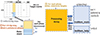 |
Figure 16. Dynamic calculating-scheduling framework [115] |
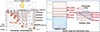 |
Figure 17. Calculating-scheduling flow and Rd/Wr cases for instruction memories [115] |
3.2.3. Review of dedicated syndrome decoding module
For modern code-based schemes like HQC, the syndrome decoding process is also required as the primary computational bottleneck for decapsulation. This task is computationally intensive and often involves operations over finite fields using specialized codes (e.g., concatenated RM and RS codes). To address this, hardware development focuses on efficiently mapping decoding routines, where the complex decoding logic is offloaded to a dedicated, loosely coupled accelerator.
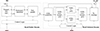 |
Figure 18. Dedicated HQC decapsulation module [98] |
(1) HQC decoding: The HQC decapsulation process is based on a custom hardware module dedicated [98] to decode the concatenated RM and RS codes. The overall architecture, shown in Figure 18, is segmented into two major stages to handle the distinct computational demands of each code. The first stage, the RM decoder (left side), is designed for efficient pattern recognition, using an expand_and_sum transformation followed by the Hadamard_transform module, which consists of seven layers of butterfly radix-2 structures to accelerate the process. Finally, the find_peaks module locates the position of the highest value to identify the decoded RM codeword components. Following the RM stage, the resulting output is passed to the RS decoder (right side), which performs the computationally intensive algebraic correction. This RS decoder implements a structured sequential workflow that is critical to recovering the original message. The process begins with the comp_syndrome unit, which calculates the syndrome vector Si, followed by the computation of the error location polynomial σ(x) and its roots (i.e., the error locations) via the comp_root module. These results are then used to determine the error values ej, allowing the fix_message unit to correct the received word and retrieve the message. This entire customized decode module ensures that the high computational complexity of concatenated decoding is managed efficiently, achieving the performance and product of the time-area superior to previous High-Level Synthesis (HLS) implementations [32] while adhering to constant-time security requirements.
(2) BIKE decoding: The BIKE decapsulation process involves a calculation-intensive process BFIter and BFMaskedIter. The customized hardware design for the BIKE decapsulation process is primarily driven by the need to accelerate the iterative Black-Gray-Flip (BGF) decoder while adhering to strict area constraints and constant-time security requirements. The state-of-the-art BGF decoder design is derived from the work [118], which is followed by the later works [119]. The decoding module is shown in Figure 19. The core computational bottleneck lies in the Bit-Flipping module, which must efficiently compute the Unsatisfied-Parity-Check (UPC) equation counts for all columns in each iteration. To achieve high throughput while conserving precious flip-flop resources, the architecture is designed to be fully scalable with the bus width parameter b, implementing b parallel counters (CNT0 to CNTb − 1) to process b columns of the error vector concurrently. The efficiency of this parallel design hinges on specialized memory management. Since the secret key (h0,h1) is stored in a compact representation (only the non-zero bit positions are stored) to minimize area, the control logic must calculate the corresponding syndrome bits for the b parallel counters simultaneously. To overcome the intrinsic sequential read limitations of BRAMs for the syndrome vector (s), the implementation employs a critical optimization: duplication of the syndrome vector (s) across multiple BRAMs (as suggested by the need to read successive bits in a non-aligned fashion). This allows the module to read the successive b bits of the syndrome required to enable parallel counters within a single clock cycle, dramatically improving the latency of the iterative decoding process. Finally, this customized module is designed for constant-time execution, ensuring that its operating time is independent of the secret key or syndrome values, thus providing inherent resilience against timing-based SCA.
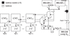 |
Figure 19. Dedicated BIKE decoding module [118] |
(3) Classic McEliece decoding: The customized hardware design for the Classic McEliece (or Niederreiter) decapsulation process is architected as a complex, constant-time algebraic decoding pipeline, designed to decode binary Goppa codes, which is shown in Figure 20. The state-of-the-art decoding module is ref. [38], which originates from ref. [117]. As shown in Figure 19, decryption is segmented into a precise sequence of specialized modules that begins by calculating the syndrome sequence based on the ciphertext and the secret key polynomial g(x). The critical first step is the evaluation module, which uses the highly specialized Gao-Mateer Additive FFT technique to perform a rapid polynomial evaluation over the finite field GF(2m), efficiently calculating the syndrome in a small number of cycles, which is fundamental to achieving a low overall latency for the decapsulation process. The resulting syndrome sequence then feeds the doubled syndrome block, which prepares the input sequence for the core algebraic decoder: the Berlekamp-Massey (BM) module. The BM algorithm, a major computational bottleneck in code-based hardware, iteratively computes the polynomial error locator σ(x), leveraging specialized GF(2m) arithmetic units that are often accelerated using Karatsuba multiplication and high-speed memory access. Finally, the roots of σ(x) are found by the Error Locator module (often another specialized Additive FFT routine for root finding), which determines the exact positions of the errors, allowing the final fix stage _message (implicitly shown) to flip the corresponding bits and output the Recovered Message. This tightly coupled, sequential pipeline is engineered to manage the finite field arithmetic and complex control flow necessary for constant-time syndrome decoding of Goppa codes.
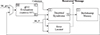 |
Figure 20. Complete McEliece decoding module [38] |
3.3. Hash-based schemes: parallel hash accelerator
Hash-based signatures, such as SLH-DSA (Sphincs+ [17, 120–122]) and the stateful XMSS/LMS, are attractive due to their reliance on highly trusted symmetric primitives (cryptographic hash functions such as SHA-256, SHAKE-256, and Chacha-20 [123]). Therefore, the computational bottleneck is also the symmetric operation, such as SHA-256, SHAKE-256, or Chacha-20. And efficient scheduling is also important to improve the utilization rate of hash cores. Therefore, for efficient Sphincs+ hardware design, two major challenges need to be addressed:
- (1)
Efficient parallel hash hardware cores;
- (2)
Efficient calculation scheduling to maximize the utilization rate of hash cores.
The efficient scheduling will be introduced in Section 4. Here, only efficient hash core designs are discussed.
Over millions of hash calls are involved in Sphincs+, therefore parallelism is easy to exploit in XMSS/FORS/WOTS+. Except for single core design [124], improving the parallel number of hash cores is the key to enhancing the hardware Sphincs+ performance. Specifically, there are three ways to improve the number of hash cores: round-parallel structure, core-based (memory-centric) structure, and core-based (register-based). The round-parallel structure, adopted by ref. [125], instantiates twelve 2-round hash cores in sequential order to complete one complete round of SHA-3 operations in the pipeline. And the core-parallel (register-based) structure, adopted by ref. [126] instantiates multiple hash cores to parallel execute the XMSS/FORS/WOTS+ operations. In addition, ref. [50] adopted a core-parallel (memory centric) structure, where different hash cores execute in parallel but share the same memory interface. The features of these three structures are summarized in Table 4. In sum, the first and third structures adapt to the dedicated hash-based PQC accelerator, while the second structure adapts to the agile PQC domain processors. Round-parallel modules save many memory accesses, while core-parallel modules (register-based) cannot.
Parallel methods of hash cores
The round-parallel SHA-3 structure is shown in Figure 21. To overcome the time overhead inherent in repeated hash evaluations, the core adopts a highly optimized unrolled and pipelined structure. The specific hardware realization of the SHAKE-256 core uses a partially unrolled pipeline architecture to achieve maximum speed while managing FPGA resource consumption. Instead of fully unrolling the Keccak permutation (which requires 24 rounds), the design strategically cuts the unrolling factor in half, implementing a 12-round pipeline that runs twice for each full permutation. This trade-off significantly reduces the FPGA logic required (saving almost 50% of resources) while still achieving high throughput. The complex control of this structure is managed by a control Finite State Machines (FSM), which orchestrates the pipeline re-entry by switching the pipeline input between the current output and a new input every clock cycle via a multiplexer (Rmux). To further maximize the efficiency of the main Sphincs+ co-processor (which handles I/O and memory), the Keccak pipeline is clocked at double the speed of the rest of the core, ensuring that the hash unit does not become a bottleneck for the signature generation process.
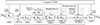 |
Figure 21. Round-parallel SHA-3 modules to accelerate Sphincs+ [125] |
3.4. Multivariate-based schemes: reusable matrix processing array
Multivariate cryptography, historically featuring schemes like Rainbow (based on the UOV construction), relies on the hardness of solving systems of multivariate polynomial equations. The computational bottleneck in this family centers on the dense matrix-vector multiplications and extensive linear algebra operations over finite fields (e.g., GF(2m)), namely matrix inversion, during signing and verification. Therefore, the bottleneck of designing multivariate-based PQC hardware is as follows: Efficient matrix hardware design (matrix inversion and related operations).
There are two main methods for designing an efficient matrix inversion in previous works [31, 85, 116, 127–129].
The works [128] instantiates a 2D processing array to execute the matrix inversion, which is shown in Figure 22. To realize a high-speed, constant-time Gaussian elimination, the design utilizes a two-dimensional Processing Element (PE) array to execute the computationally intensive steps in parallel. The linear system solver, as shown in the top-level diagram, is designed as an array n × (n + 1) of uniform n × (n + 1) PEs, where n is the size of the system (the number of variables). This parallel structure is designed to execute each iteration of the Gauss-Jordan elimination algorithm in a single clock cycle, achieving a fast solution time of n clock cycles for an n × n system. The data flow direction follows from the top to the bottom, where in each row the linear operations are executed between the input vectors and the data stored in this row. When the input data are finished, the entire matrix has been eliminated. Crucially, the system incorporates a novel PivotCalc module that calculates the pivot row index without requiring row swapping, which is essential to prevent the timing of a side-channel leak during the system solution process. This parallel reused matrix processing array provides a low-latency method to handle the core algebraic bottlenecks of multivariate PQC.
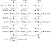 |
Figure 22. 2D array-based matrix inversion hardware [128] |
The work detailed in ref. [31] presents a hardware accelerator design that uses a reusable processing array coupled with a dedicated scheduling algorithm for matrix elimination, as illustrated in the left portion of Figure 23. For a matrix of size L × K, the overall Gauss elimination process is partitioned hierarchically: divided into ⌈L/v⌉ phases, and each phase is subsequently broken down into multiple steps, where v represents the vector processing length. This organizational structure for phases and steps aligns with the method established in ref. [37]. The hardware includes two separate memory blocks dedicated to storing structural metadata: one for the re-organized row order and another for the necessary scaling vectors. The input data matrix itself is segmented into multiple column blocks. During the first step of any phase, one complete column block of data is processed entirely to its final, eliminated form. This completed processing is then replicated on the remaining column blocks in all subsequent steps of that phase. Execution within a step involves two nested processing loops. In the first step of each phase, the system searches for a pivot row (a row with a non-zero pivot value). Once a pivot is identified, that row is selected as the pivot row, a normalization process is immediately executed, and its row index and normalization factor are recorded in the dedicated storage blocks, respectively. If the current input row is not selected as the pivot row, the system executes the corresponding elimination operation using the element at the pivot’s location in the input row as the scaling factor. For any step after the first one, the system simply retrieves the required pivot row index and obtains the necessary scaling factors. This eliminates the need to recalculate or re-identify these values.
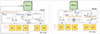 |
Figure 23. Reusable array-based matrix inversion hardware [31] |
Feature comparisons between two major matrix hardware structures are shown in Table 5. The 2D array-based matrix inversion hardware requires one inversion hardware in each row and will be difficult to reuse for other objectives. Using data re-use, the number of memory accesses can be reduced to very low. Comparatively, 1D reconfigurable array-based has high reconfiguration, but it requires frequent memory accesses.
Feature comparisons between two major matrix hardware structures
The Multiplication-Accumulation Operation (MAO) module presented in ref. [31], which is shown in the right side of Figure 23, is designed to handle both three-dimensional matrix operations and large-scale matrix-vector operations over the Galois Field GF(2). Both types of matrix operations are implemented via vectorized multiplication and accumulation. The operational sequence begins with loading an initial vector into the result buffer, Rvec. Subsequently, scaled vectorized multiplications are performed between a newly read input vector and a coefficient retrieved from Rvec. The resulting products are then accumulated directly back into Rvec within the MAO module, and this multiplication-accumulation process is repeated as dictated by the configuration. The MAO module offers significant flexibility through various configuration options. Specifically, the design allows for pre-multiplication of the input vector by a constant before processing, as well as configuration of the result buffer’s initialization state. Furthermore, the memory access patterns, including the memory address stride and the starting address of Rvec, are fully configurable, ensuring broad adaptability for the module.
3.5. Isogeny-based schemes: Dedicated optimized reduction module
Isogeny-based cryptography, most notably SIKE (now broken), cSIDH, and ongoing work on SQIsign, is distinct, as it is the only major PQC family whose core operations still rely on long-integer modular arithmetic, similar to classical ECC and RSA. The security depends on the complex relationships between elliptic curves. Therefore, the hardware design principle is relatively similar to that of ECC hardware [130–134], dedicated large-size modulus hardware is needed in Isogeny-based PQC accelerator [135–139].
Most of the research on SIKE hardware focuses on the optimization of the reduction hardware based on the special modulus values, which is just shown in Figure 24.
 |
Figure 24. Efficient Montgomery reduction unit in SIKE hardware [140] |
Implementing these large-integer operations efficiently requires a dedicated optimized reduction module tailored specifically for multi-precision modular multiplication and reduction. Techniques like Montgomery multiplication are critical to accelerating these operations. The focus is on designing the ALU and the data path to handle these specific large-integer operations efficiently. As depicted in Figure 24 (Montgomery Multiplication Architecture Proposed), the design adopts a dual multiplication architecture, allowing the core to perform two multiplication operations simultaneously within each cycle to maximize throughput. The primary innovation lies in exploiting the special form of the SIKE prime (p = 2A × 3B − 1), which allows the design to streamline the computationally expensive modular reduction process. The entire architecture is partitioned into several pipelined blocks–including PE Initial, sA-Mult, and sB-Red blocks, which are meticulously scheduled to reduce the critical path delay and minimize resource consumption.
This segmented and pipelined approach achieves its efficiency by intelligently handling the arithmetic flow. The design splits the multiplication-reduction steps into two parts, using the observation that in the first portion of the prime (p[j]), the words are all ones, allowing the architecture to skip unnecessary multiplication-reduction operations in the sA-Mult phase, thus saving clock cycles and complexity. Data propagation is rigorously controlled: the PE Initial block calculates the first carry C and the quotient m (the reduction carry Cr), where C is propagated forward through the multiplication path, while the S result chunk is propagated backward to be stored in the previous result chunk T[j − 1]. The details of the optimized dedicated Montgomery reduction can be found in ref. [140]. This intricate scheduling ensures that the PEs are continuously utilized, allowing the high clock frequency of the logic core to dominate the overall performance, making the SIKE implementation highly competitive on FPGAs.
4. Hardware platforms of PQC and design paradigms
The implementation of PQC algorithms requires careful selection of hardware platforms to balance flexibility, performance, energy efficiency, and cost. As PQC standards evolve, supporting diverse mathematical problems such as lattices, codes, and hashes, the choice of platform becomes critical. This section explores four primary implementation platforms: general-purpose processors with PQC ISEs, FPGAs, ASICs, and DSAs, detailing their architectures, advantages, limitations, and specific applications in PQC. Each platform offers unique trade-offs, influencing their suitability for various use cases, from high-performance servers to resource-constrained IoT devices. The analysis draws on recent research and hardware implementations to provide a comprehensive overview of the current landscape.
4.1. General-purpose processors and PQC-ISEs
The successful migration of PQC hinges on its efficient integration with the vast existing ecosystem of General-Purpose Processors (GPPs) [32–35, 141], particularly in ubiquitous platforms like embedded ARM Cortex-M micro-controllers and flexible RISC-V System-on-Chips (SoCs). Although PQC algorithms such as ML-KEM (Kyber) and ML-DSA (Dilithium) impose a substantial computational load–characterized by high-degree polynomial and matrix arithmetic–the strategy of full software execution often fails on resource-constrained GPPs. Consequently, the incorporation of PQC ISEs into the host CPU has emerged as the prevailing design paradigm for accelerating PQC. This methodology uses some PQC-dedicated instructions to offload complex PQC primitives directly into specialized logic units, achieving efficiency while retaining the critical flexibility afforded by software control.
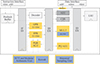 |
Figure 25. Tightly-coupled PQC architecture [141] |
The design and merge of ISEs into mainstream general GPPs involve the tightly-coupled co-design and synchronization methodology. The implementation of PQC via custom ISEs embodies a tightly-coupled hardware-software co-design approach where the functional units are strategically partitioned. The host GPP manages complex control flow, data scheduling, and system orchestration, while the ISEs serve as the crucial dedicated module to delegate high-arithmetic operations. This tightly-coupled structure merges the PQC ISE modules into the instruction pipeline. This synchronization model minimizes latency through the processor pipeline: the GPP issues a custom PQC instruction, which triggers the hardware module to execute the complex computation (e.g., an NTT butterfly unit operation). Upon completion, the result is returned directly to the GPP’s registers or dedicated PQC processors, avoiding the latency and overhead associated with complex bus communication or memory-mapped I/O during the critical path operation itself. This precise functional partitioning drastically reduces the execution cycle count for PQC primitives, thereby minimizing the overall energy and time-area product of the system. The tightly-coupled architecture is depicted in Figure 25.
As depicted in Figure 25, The integration of PQC in GPPs is performed most effectively through tightly-coupled ISEs [141]. This work introduced an enhanced RISC-V architecture that pioneered the deep integration of specialized accelerators–eliminating the high data transfer overhead inherent in prior loosely-coupled designs. The architecture modifies the standard pipeline (IF/ID/EX) with custom logic, including a Post-Quantum Register ALU (PQR-ALU); the PQR-ALU, located in the Decoding Stage, integrates the NTT and Modular Arithmetic Unit and the Keccak Accelerator to enable parallel, low-latency access to the existing General and Floating Point Register Banks. The system was extended with approximately thirty new instructions to directly command operations such as packed modular arithmetic, butterfly computations, and efficient polynomial sampling via the Binomial Sampling Unit. Implemented for lattice-based schemes like NewHope, Kyber, and Saber, the co-design achieved significant quantitative results.
The work [34] demonstrated an optimized hardware-software co-design for Kyber and Dilithium on a RISC-V SoC FPGA platform. The open nature of the RISC-V architecture makes it highly suitable for custom ISEs. The architecture utilized a unified high-level architecture and custom instructions to accelerate core polynomial arithmetic operations through specialized hardware modules. This tight integration, combined with the optimization of the RISC-V assembly for supporting functions such as hashing, resulted in a substantial improvement in 3× to 5× overall performance across security levels, while the hardware accelerators consumed less than 5% of the total FPGA resources.
The work [35] explored how the ISE paradigm facilitates taking ML-KEM and ML-DSA from the ARM Cortex-M4 to the Cortex-M7 architecture. The ISE strategy is critical for achieving micro-architectural agility on deeply embedded platforms. This research demonstrated the essential role of custom instructions in maintaining implementation efficiency across different micro-architectures without requiring a complete redesign, proving that the ISE is the necessary abstraction layer for rapid deployment.
The work [32] implements accelerated code-based cryptography through PQC ISE for memory-intensive algorithms such as HQC. The utility of PQC ISEs extends beyond lattice schemes, providing the necessary algorithmic flexibility to handle the diverse PQC families; the approach has been validated through a co-design that explored tightly coupled hardware acceleration by instruction set extension. This partitioning allowed the acceleration of linear bottlenecks and the complex syndrome decoding process, demonstrating how ISEs can be tailored to accelerate bottlenecks that are fundamentally different from lattice-based NTT arithmetic. The implementation of a code-based ISE [33] was even developed to protect Boolean masking in software, showcasing the role of custom instructions in bridging functional speedup with implementation security.
Besides, General-Purpose graphics processing units (GPUs) have emerged as a pivotal platform for achieving high-throughput acceleration through massive parallelism, especially given their high computational demands.
Recent research has demonstrated significant performance gains across various NIST-standardized algorithms. For KEMs like Kyber, GPU acceleration [142, 143] focuses heavily on the NTT module, where optimizations such as refined thread arrangement in butterfly patterns are employed to minimize memory access overhead. Similarly, for CRYSTALS-Dilithium [143, 144], GPU-centric designs prioritize NTT, polynomial arithmetic, and random sampling, achieving substantial speed-ups in signature generation and verification through efficient batch processing.
Beyond lattice-based schemes, BIKE–a code-based KEM has been optimized through frameworks like ECO-BIKE [145], which introduces parallel dense polynomial multiplication and refined XOR calculations to bridge the implementation gap on GPU architectures. Furthermore, digital signature schemes such as Falcon face unique challenges due to the complexity of Fast Fourier Sampling. Advanced implementations like cuFalcon [146] and GOLF [147] address these via adaptive parallel strategies and specific FFT enhancements, setting record-breaking throughput levels. Collectively, these developments underscore the feasibility of utilizing GPUs to mitigate the computational bottlenecks of PQC in high-demand environments.
In high-concurrency environments like cloud infrastructures, GPUs excel at throughput-oriented tasks such as batch key generation and large-scale signature verification. However, inherent overheads from host-to-device data transfer and kernel launches render GPUs less effective for latency-sensitive, single-operation responses. Additionally, the high power consumption and hardware acquisition costs pose substantial barriers in cost-constrained or resource-limited edge scenarios. Consequently, while GPUs are ideal for high-demand servers, more energy-efficient or specialized hardware accelerators remain more viable for localized and budget-sensitive applications.
In conclusion, the seamless integration achieved through PQC ISEs enables GPPs to serve as robust platforms for the PQC transition. This methodology provides a path to low-overhead, low-power PQC deployment across a wide range of architectures by mapping complex algebraic operations to dedicated, instruction-controlled hardware logic, thereby maximizing performance while preserving architectural flexibility.
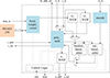 |
Figure 26. FPGA-based HQC accelerator [98] |
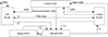 |
Figure 27. FPGA-based Sphincs+ accelerator [124] |
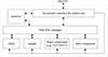 |
Figure 28. FPGA-based lattice accelerator [36] |
 |
Figure 29. FPGA-based BIKE accelerator [118] |
4.2. FPGA-based PQC accelerator
FPGAs represent a versatile middle ground between the flexibility of software and the efficiency of hardware, making them an important platform for PQC implementations that require high performance and deployment speed [148, 149]. FPGAs consist of configurable logic blocks, programmable interconnects, and embedded resources such as block RAMs and DSP slices, which can be reprogrammed post-deployment to implement custom digital circuits tailored to specific PQC algorithms. This reconfigurability allows designers to map PQC algorithms to a dedicated FPGA architecture with adaptability to the specific BRAM and DSP structure [36, 39–42, 91]. Create deep pipelined parallel architectures that significantly outperform software running on general-purpose processors, achieving relatively high throughput for algorithms like Kyber by leveraging parallel NTT units and optimized datapaths, which has been introduced in Section 3.
Figures 26–29 show the FPGA-based accelerator that supports HQC, Sphincs+, lattice-based PQC and BIKE, respectively. The overall architecture of FPGA-based PQC accelerators is uniformly characterized by a memory-centric design approach, where specialized arithmetic units are constructed around high-speed on-chip memory banks [150] to mitigate the significant data transfer overhead and high storage pressure inherent in PQC schemes. The key bottleneck and dedicated data-path modules have been introduced in Section 3. Across all four distinct families–lattice, code, and hash-based-the core functionality is dictated by a central control unit that is typically implemented as a complex FSM responsible for precise data orchestration. For the generic lattice-based accelerator [36] shown in Figure 28, the FSM directs the data flow between the central memory and specialized functional units such as the NTT/ ITT and Hash blocks, ensuring efficient scheduling for polynomial arithmetic. Similarly, the BIKE accelerator [118] shown in Figure 29 features a master FSM that coordinates the sequencing of its polynomial multiplier and inversion modules with the central Memory Bank for iterative decoding, leveraging the register bank to store intermediate results and key components. The Sphincs+ accelerator shown in Figure 27 utilizes a specialized Control unit to manage sequential, memory-intensive hash-chaining operations, dictating the flow between the SHAKE-256 engine, the Cache RAM (for MT nodes) and the Mask FIFO, providing a high-speed core essential for stateless signing. Finally, the HQC accelerator [98] shown in Figure 26 is architected as a functional pipeline where the control logic coordinates the sequential algebraic decoding steps, ensuring the correct transfer of data between the RM Decoder and the RS Decoder via memory banks (r1 RAM, r2 RAM), using poly_mult and specialized adders to handle the arithmetic of GF(2) necessary for concatenated decoding. This pervasive reliance on FSM-based control over shared memory resources is essential to achieve the high throughput of the FPGA-based PQC accelerator.
A key strength of FPGAs lies in their support for cryptographic agility, as the same physical device can be reconfigured to support different algorithms or updated versions through bitstream modifications. This is crucial for long-term security in the quantum era, as it allows systems to adapt to new threats without requiring hardware replacements. The ability to dynamically reconfigure FPGAs via bitstream updates enables cryptographic agility to some degree with a relatively long reconfiguration time. This method also ensures that hardware investments remain future-proof against algorithmic changes or breakthroughs, such as those arising from NIST’s ongoing standardization process. This makes FPGAs particularly valuable for transitional phases where multiple PQC schemes may need to be supported simultaneously and for new PQC schemes that need fast deployment.
Design methodologies for FPGAs often involve HLS tools, such as Xilinx’s Vitis HLS [151] or Intel’s Quartus HLS [152], which enable designers to describe functionality in high-level languages like C++ or System C, automatically generating efficient Register-Transfer Level (RTL) code for PQC kernels such as polynomial multiplication, sampling, or hashing. Additionally, FPGA designs can be parameterized to support various security levels (e.g., Kyber-512, Kyber-768, Kyber-1024) and algorithm parameters, enhancing their versatility across different use cases. For instance, a single FPGA design can be tailored to handle both lattice-based algorithms like Dilithium and code-based schemes like Classic McEliece by dynamically loading appropriate bitstreams, reducing development overhead and improving time-to-market.
Despite these advantages, FPGAs typically consume more power and have higher per-unit costs compared to ASICs [153], due to the overhead of programmable routing, configuration memory, and general-purpose logic. Power consumption can range from 1 W to 10 W [154] depending on design complexity, clock frequencies, and resource utilization, which can be prohibitive for battery-operated devices such as IoT sensors or mobile handsets. Moreover, FPGA development requires specialized expertise in hardware design, including RTL proficiency such as Verilog, as well as knowledge of timing closure, place-and-route optimization, and power management, leading to longer development cycles and higher initial costs. However, for mid-volume applications, such as network appliances [155], research prototypes [156], or industrial control systems [157], FPGAs offer an excellent balance of performance and flexibility, allowing rapid prototyping and customization without the Non-Recurring Engineering (NRE) costs associated with ASICs.
Recent advances in FPGA technology are further improving their efficiency and usability for PQC implementations. For example, the integration of hardened IP cores for common PQC operations, such as SHA-3 for hashing or Keccak accelerators [158], reduces resource usage and power consumption while enhancing performance. Modern FPGA families, such as Xilinx’s UltraScale+ [159] or Intel’s Agilex [160], feature enhanced DSP blocks and High-Bandwidth Memory (HBM), which are ideal for data-intensive PQC operations such as large polynomial multiplications. Tools such as Xilinx’s Vitis [151] and Intel’s Quartus Prime [152] enable faster design iteration, optimization, and verification through features such as automated floor planning and real-time power analysis. In practice, FPGA-based PQC implementations have demonstrated better energy efficiency than software on CPUs, making them suitable for edge computing and partial cloud computing, and embedded systems where low latency and moderate power budgets are critical.
4.3. Specific PQC hardware accelerator (ASIC)
Unlike FPGA-based PQC accelerators, dedicated PQC ASICs need to push hardware performance to the extreme. Therefore, ultra-optimization in data-path and memory organization need to be considered during design ASICs.
We take ref. [86] as an example, Figure 30 illustrates the core architectural concept of a high-performance ASIC accelerator designed for lattice-based PQC, such as the CRYSTALS-Kyber KEM. The design philosophy focuses on maximizing parallelism for computationally intensive polynomial multiplication operations while employing a sophisticated control structure for efficient data management and sequencing.
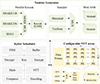 |
Figure 30. Kyber-specific ASIC [86] |
The design is modularized into three main functional areas: the central control structure, the random number generation unit, and the parallel computation core.
- (1)
Control Structure Design: The entire PQC operation sequence is managed by the Kyber Scheduler, which serves as the central control structure. This scheduler contains an FSM that directs the high-level KEM procedures (Keygen, Encrypt, and Decrypt). The scheduler orchestrates the flow of data through necessary low-level functional blocks, including Hash, NTT, Compress, and Encoding modules. Effective control is essential because PQC algorithms involve data-dependent operations and complex state transitions that must be executed in a specific, often constant-time, sequence to ensure security. The adjacent operations need to be scheduled to achieve both parallelism and correctness.
- (2)
Number Generator: Provides the necessary cryptographic randomness, integrating a Parallel Keccak core (supporting SHAKE-128, SHAKE-256, and SHA-3) and specialized Sampler blocks (Binomial and Uniform) for generating the required noise polynomials.
- (3)
Storage and Computation Organization: The hardware’s high-speed capability is vested in the configurable NTT array for the engine for polynomial arithmetic, which is the primary bottleneck for lattice-based schemes. This core consists of a highly parallel array of PEs, designed to execute the NTT and its INTT, along with other arithmetic modes. The array’s configurable nature allows it to be efficiently reused across different sub-operations and security levels. The Storage Organization reflects a critical optimization strategy for PQC: addressing the memory bottleneck. The design utilizes efficient buffer Storage: The Kyber scheduler incorporates a Buffer for temporary storage and swift exchange of intermediate polynomial coefficients between the control unit and the computation core. This architectural choice drastically reduces latency and energy consumption by minimizing the movement of large data volumes–such as polynomial coefficients–away from the memory and closer to the processing unit.
In sum, the organization of memory and the bit width of the data paths need to be finely adjusted to adapt to the algorithm parameters and minimize hardware resource overhead, unlike the FPGA-based design. The existing works are listed in Table 6.
The existing PQC ASICs
Figure 31 summarizes silicon-proven PQC hardware comparisons, illustrating current state-of-the-art trade-offs with respect to performance, flexibility, and energy consumption in ASIC. The left part, Throughput vs. Energy Efficiency, demonstrates that modern PQC accelerator designs have conquered the initial challenge of high computational overhead. Recent high-end architectures (e.g., VLSI’25 [163] and TCAS-II’25 [164]) have successfully pushed peak throughput close to 90 thousand operations per second (KOPS) while maintaining excellent energy efficiency, clustered within the ultra-low range of 1–3 micro joules per operation (μJ/OP). The work [163] proposed a RISC-V extension accelerator with high parallel butterflies to support FIPS 203/204/205. The accelerator [164] presented a computing-in-memory accelerating macro to support NTT operations. The agile PQC DSAs [50, 85] proposed memory-centric and task-pash-based architecture to support multiple mathematical problems. The previous work [89] utilized a serial configurable ALU to incorporate the lattice-based schemes. Besides, the works [161, 162] adopted the dedicated architecture for some specific schemes. This clustering at low energy cost is a significant achievement, indicating that architectural optimizations, such as parallelized NTT engines and efficient memory access, have effectively eliminated energy inefficiencies seen in older implementations (e.g., ISSCC’19 [89] at over 80 μJ/OP), making high-speed, low-power PQC deployment feasible for applications from data centers to embedded systems. The right graph, Throughput vs. Existing Supported Schemes, highlights the critical role of functional flexibility in the PQC transition period. Although the fastest designs (VLSI’25 [163]) tend to support a moderate number of schemes, designs focused on maximum flexibility (e.g., ISSCC’24 [50]) successfully support up to 8 different PQC algorithms or security levels, maintaining a highly competitive throughput of approximately 70 KOPS. This shows that the performance penalty for implementing unified, multi-scheme PQC accelerators has become negligible. This high degree of flexibility is essential for real-world adoption, allowing hardware platforms to simultaneously support multiple NIST standards (such as Kyber for KEM and Dilithium for DS) and easily adapt to future cryptographic evolution without requiring a costly redesign of the silicon.
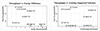 |
Figure 31. Silicon-proven performance comparisons (Throughput vs. Energy efficiency; Throughput vs. Existing Supported Schemes.) |
The future trend for PQC ASIC development is thus focused on creating highly unified architectures that achieve both high energy efficiency and maximum flexibility to support evolving PQC standards.
Interestingly, existing research concerning the chip-level verification of non-lattice-based primitives remains limited. This gap is primarily a consequence of the nature of the current standardization landscape, which has historically deterred large-scale ASIC investments. However, as the field matures, this domain is rapidly evolving into a critical avenue for future exploration. Specifically, the hardware realization of the newly standardized HQC algorithm is gaining substantial momentum, positioning it as a prominent topic within the hardware security community.
4.4. Agile PQC DSA
As mentioned above, GPP is limited by its performance and energy efficiency, while FPGA also lacks its ability to achieve extreme power efficiency. In addition, FPGA’s long reconfiguration time also hinders its agility in the real scenario. The specific ASIC can achieve the best latency and energy efficiency, which was focused only on one or a specific family of PQC algorithms. In many real-world applications, ASIC platforms do not meet the requirement of multiple algorithms.
Therefore, to balance performance and agility, DSA is more suitable for PQC deployment, especially in the cloud server. The newest PQC DSAs [50, 85] support three different mathematical problems. According to these two studies, the core design bottlenecks are summarized as follows:
- (1)
Agile and efficient control and scheduling mechanism, such as dynamic-updated PQC task path;
- (2)
Efficient calculation architecture and reusable multiple-field processing array;
- (3)
Complete and reconfigurable PQC calculation operators.
To address these challenges, efficient PQC operators discussed in the third section, including NTT, inversion, hash, and other modules, are aimed at the third challenge. The subsection will introduce the current methods for the first two challenges.
4.4.1. Complex PQC scheduling and control logic
To efficiently schedule the task operators on the PQC chip, the scheduling module must manage the dependency automatically. In addition, static scheduling requires mapping branch operations and loop behavior. The control module also needs to manage the data-dependent tasks and communication with the main buffer.
The core of this agile PQC chip [50] is a highly parallel and dynamically managed architecture, built around several clusters of specialized operators. To aggressively minimize memory port contention, operators with identical functions are forcibly grouped into clusters, specifically: the Hash Cluster, Sample Logic Cluster, Arithmetic Cluster, Format Logic Cluster, and Communicate Cluster. Each cluster is armed with a set of configuration registers that are fully reusable by all embedded operators, with the register bits providing auxiliary operands beyond the immediate running tasks.
The system’s control hinges on a four-stage task-path: Task memory (Taskmem), Task Fetcher, Task Updater, and Task Scheduler. Execution is initiated by storing tasks in Taskmem, from which the Task Fetcher reads them, meticulously managing the Program Counter (PC) and handling all jump operations. To mitigate pipeline stalls, the Fetcher is equipped with a FIFO to buffer pre-read tasks. Furthermore, Fetcher enforces the correctness through a lock mechanism designed to prevent the retrieval of obsolete tasks that are about to be overwritten by a Mem2taskmem (M2T) communication task. This lock is activated by the M2T task and is released only upon completion, with the fetch FIFO being forcibly reset upon receiving a jump signal or detecting a collision with the soon-to-be-overwritten memory region.
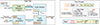 |
Figure 32. Dynamically-updated task path in ref. [50] |
As shown in Figure 32, every task is prefixed with control bits that allow dynamic running time modification. These prefix bits designate the Updater registers to be used and indicate whether the current task requires modification. There are four critical task types that dictate the system’s function.
- (1)
Run-Task: Executes a task operator (the actual computation).
- (2)
Config-Task: Sets the configuration registers within an operator cluster.
- (3)
Update-Task: Manages the internal update registers of the Task Updater.
- (4)
Communicate-Task: Moves data between buffer (BUF), MEM, external interfaces, and Taskmem.
The Task Updater is a pivotal component, recalculating the task’s address and length segments based on its internal registers. The source, destination, and length segments are dynamically modified by adding or subtracting values from configurable register values. The Updater utilizes two classes of registers–static (input-independent) and dynamic (data-dependent, fed by the Buf2Updater (B2U) task)–each having two sets of registers (one 32-bit and three 10-bit). The Updater can be configured via the Update-type tasks to perform four distinct update operations (+, −, ×, or replace), and these tasks can manage register-to-register operations and branching internally. Crucially, this allows Run-type task modifications to occur in parallel with operator execution. A specific lock mechanism is also implemented here to ensure correctness: when a B2U task is scheduled, the WaitB2U flag is raised, suspending the pipeline until the B2U task completes if the subsequent task depends on the dynamic registers being updated.
The Task Scheduler is the final gatekeeper, utilizing a FIFO issue to buffer tasks awaiting dispatch. Its central function is a rigorous dependency check between tasks in the buffer and those currently running. Only when all dependencies are cleared is a task issued. This check is highly complex, covering address collisions within BUF/MEM, cluster conflicts, and control dependencies (such as Run-Task vs. Config-Task). Since tasks specify multiple address regions, specialized circuitry is required to detect region-based conflicts.
The design leverages maximal parallelism: Run-tasks can execute concurrently with other Run-tasks, Config-tasks, Communicate-tasks, and Update-tasks. Furthermore, PQC schemes often involve streaming data access, where addresses increment by one per cycle. This streaming flag enables aggressive Read-After-Write (RAW) hazard mitigation: the results of an operator can be immediately forwarded to the next operator without waiting for the entire preceding task to finish. The scheduler uses a streaming flag and a wr_begin signal to bypass standard RAW checks, minimizing overhead.
In conclusion, this dynamically-updated task-path fundamentally satisfies the control demands of a general PQC accelerator. Robust data-dependency maintenance is enforced by a region-correlation-based scheduler, while data-related tasks and memory interaction are handled by the dynamic Task Updater. Control flow correctness is further guaranteed by multiple lock mechanisms. Future work should extend this potent control paradigm to all cryptographic and mathematical problems.
4.4.2. Multi-field reconfigurable array and configuration mechanism
A critical bottleneck in designing an agile PQC chip is the creation of a universal, general-purpose data-path capable of supporting the wildly diverse mathematical problems inherent in PQC. This demands radical support for various types and sizes of rings, fields, and groups. The immediate, non-negotiable solution is a reconfigurable arithmetic array.
The architecture in ref. [50] demolishes this bottleneck by proposing a hierarchical framework built for multi-scheme PQC support.
- (1)
Algorithm-Level: The highest level, where all complex executions are broken down into simpler task-level or coefficient-level operations.
- (2)
Task-Level: Here, the system executes coarse-grained tasks such as NTT, Vectorized-AE (VAE), and FFT. These tasks offload all linear multiplication-type operations directly to the arrays AE and Floating-Elements (FE), optimizing and accelerating the algorithmic bottlenecks.
- (3)
Coefficient-Level: The lowest level that directly supports the triple-field operations executed by the dedicated AE and FE arrays.
This framework aggressively balances performance and flexibility with area consumption. Optimized coarse-grained tasks drive performance, while fine-grained operations provide necessary flexibility. Crucially, reusing the costly AE and FE arrays dramatically reduces the overall area overhead. The Arithmetic Cluster is the computational heart, hosting the AEs, FEs, task operators, configuration registers, and a vital Arithmetic Cache. This cache is instantiated specifically to mitigate the bandwidth limitations often imposed by costly crossbar connections between the main data BUF and the execution unit. By pre-loading constants, particularly the twiddle factors for transforms, the cache provides exceptionally high data bandwidth. It is segmented into four banks, each with 128-depth and 512-width.
To handle the immense computational load, the cluster incorporates a massive AE array (divided into 32 elements) and an FE array (composed of 8 elements). Each FE is a potent engine, containing four double-precision float multipliers capable of executing a full complex field butterfly operation.
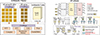 |
Figure 33. The architecture of arithmetic cluster and reconfigurable arithmetic element [50] |
The core idea lies in the reconfigurable design of the AE and FE modules, as illustrated in Figure 33. The AE is a hybrid powerhouse, structured in three stages–Pre-Add, Mul-stage, and Post-Add–and fuses butterfly operations with Karatsuba-based number multiplication. The FE focuses exclusively on float-related calculations, transferring 64-bit integer multiplication to the AE. Both AE and FE can be instantly configured for various working modes, including common butterfly and generic linear operations. This reconfigurable architecture is the key solution that simultaneously reduces area overhead and increases hardware efficiency. The NTT and FFT modules exemplify this reuse: they share an almost identical architecture, comprising an input permutation (for the inverse transform), butterfly operations executed in the AE or FE arrays, and an output permutation (for the forward transform). Twiddle constants are accessed from the high-bandwidth arithmetic cache. This design enforces an in-place topology–the writing address matches the reading address for each iteration, a strategy adopted from ref. [31] and extended here to the FFT–which optimizes network complexity.
In final summation, to decisively bridge the vast gap between high-level PQC mathematics and low-level finite field operations, this hierarchical framework is essential for narrowing the scope of hardware design. The evolution of the reconfigurable AE design, from ref. [31] to the highly advanced iteration in ref. [50], provides the foundational, field-agnostic support that future works should immediately adopt and extend.
4.5. Feature comparisons among different platforms
Based on the discussion above, this subsection will introduce the features of different PQC platforms. The hardware implementation landscape for PQC is defined by a sharp trade-off between adaptability and raw performance. Software running on Instruction-Driven Processors [32–35] offers the highest functional flexibility, but at a severe cost: throughput is minimal (20 ∼ 1000 OPS), and latency is high (1 ms ∼ 50 ms). In contrast, Custom ASICs [96, 162, 163] deliver the highest performance, with throughput reaching 85 KOPS and superior energy efficiency (30 K ∼ 500 KOps/J) at low latency (10 μs ∼ 100 μs), where 1 Op denotes the whole scheme including key generation, encapsulation (signature generation), and decapsulation (verification). However, this specialization results in inherently low functional flexibility, making it difficult and costly to update as the PQC standards evolve. Reconfigurable programmable chips, such as FPGAs, provide a middle ground, offering relatively high functional flexibility and improved physical security at intermediate performance levels.
The architecture of the DSA [31, 50] within the reconfigurable category represents the optimal platform to implement a flexible PQC solution. DSAs successfully bridge the gap between ASIC speed and programmable flexibility. They achieve the lowest latency of all hardware options (15 μs ∼ 250 μs) and the highest peak throughput, up to 65 KOPS. This combination of ultra-low latency and robust energy efficiency (20 K ∼ 220 KOps/J) makes DSAs ideal for high-frequency operations like digital signing and verification. Crucially, DSA retains the relatively high functional flexibility and security of programmable chips, ensuring that the PQC DSA implementation can be rapidly updated to comply with future NIST standards or new security countermeasures without requiring a costly and time-consuming custom silicon redesign.
5. Potential quantum attack and agile hardware defenses
Although PQC has rapidly emerged, the focus is on developing new mathematical problems believed to be difficult for both classical and quantum computers. However, PQC algorithms themselves are not immutable; their security remains under constant scrutiny from both classical and quantum cryptanalysis, highlighting the crucial need for a review of PQC hardware design.
This section first delves into the landscape of potential quantum attacks against PQC schemes, reviewing the critical vulnerabilities discovered in various leading algorithms. Subsequently, PQC schemes based on the novel security assumptions are introduced that do not rely solely on currently popular hard problems. Finally, it details the concept and implementation of agile hardware defense and multiple mathematical problem backup. This strategy advocates for a hardware design capable of rapidly migrating and updating cryptographic primitives based on different mathematical foundations, ensuring the system can quickly migrate to a secure alternative when the underlying hard problem of a deployed PQC algorithm is compromised.
5.1. Potential quantum attack
Despite the fact that the PQC field is still developing, several high-profile candidates have been broken by classical cryptanalytic attacks.
In particular, the SIKE scheme [68], a 4-round candidate in the NIST standardization process, was completely broken by an efficient classical key-recovery attack leveraging auxiliary points [70]. It exploited auxiliary points on super-singular elliptic curves to find a short vector, leading to a complete break of SIKE’s security within hours. Similarly, the Rainbow multivariate quadratic signature scheme, a candidate in the third round, was also successfully attacked [165]. It exploited the inherent algebraic structure of the algorithm, transforming the signature problem into an easily solvable linear algebra problem.
Furthermore, even algorithms based on the assumed security of lattice problems, which form the basis of the majority of standardized PQC schemes, have faced significant theoretical challenges. And recent advances documented in the LWE Challenge Hall of Fame and follow-up analyzes [166, 167] demonstrate that solving LWE instances is progressively more efficient. Improved combinatorial and lattice-reduction algorithms–especially refined dual/primal attack models–have reduced the concrete security of standard LWE parameters by several bits. These improvements directly impact structured variants such as Ring-LWE and Module-LWE, since their effective lattice dimensions and attack cost slopes differ from unstructured LWE assumptions [166]. Consequently, the “full-bit" security of such schemes must be recalculated using updated cost models. Recent reassessments indicate that Kyber-512, which targets NIST Level 1 (AES-128), may lose part of its security margin when these newer attacks and more realistic cost estimates are considered, potentially dropping below the recommended threshold. Although no practical break has been published, the narrowing margin underscores the importance of using Kyber-768 or larger parameters for long-term deployments.
Recent attacks on LWE problems [168] present a novel quantum approach to solving the LWE problem in polynomial time, marking one of the most conceptually significant attempts to challenge the assumed hardness of lattice-based cryptography. Their algorithm explores an innovative combination of quantum Fourier sampling and structured noise analysis, aiming to exploit hidden algebraic relations within LWE instances. This approach provides valuable theoretical insight into how quantum resources might interact with the noise structure that underpins the security of LWE. However, despite its ingenuity, the method ultimately does not constitute a practical or complete attack of the LWE problem: the key assumptions required by the algorithm remain unproven or unrealizable for general parameter settings. As such, while the result opens promising directions for future quantum algorithm research, it does not undermine the current post-quantum security claims of LWE-based schemes, but rather enriches the future attack methods of LWE-based schemes.
And the recent famous attacks on PQC algorithms are listed in Table 7.
Recent attacks on PQC schemes
5.2. The support of PQC algorithms without hard problems
Most of the candidates in the NIST PQC standardization process, such as CRYSTALS-Kyber and Dilithium, rely on the conjectured difficulty of specific mathematical problems, primarily those related to lattices. However, the unexpected breaks of schemes like SIKE and Rainbow underscore the potential fragility of complexity-based security assumptions, especially as cryptanalysis evolves in the quantum era. To mitigate the risk of systemic failure should a major hard problem be compromised, robust cryptographic systems must incorporate backup algorithms whose security is not predicated on unproven mathematical intractability. This necessity has driven renewed interest in cryptographic families that derive their security from more established primitives, specifically Hash-based Signatures [17] and MPCitH Signature Schemes [169], which offer an essential layer of foundational security and backup alternates to resist future quantum attack.
Hash-Based Signatures, exemplified by stateful schemes like XMSS and stateless schemes like Sphincs+, are constructed solely from secure collision-resistant hash functions and one-time signature schemes (like Lamport or Winternitz). Their security is rooted in the proven quantum-resistance of the underlying symmetric primitives (e.g., SHA-256 or SHAKE-256), which only suffer a minor security reduction from Grover’s algorithm–a threat easily countered by doubling the output size. Hardware implementation [125, 170] is relatively straightforward, mainly requiring efficient symmetric cryptography accelerations and optimized logic for MT traversal and state management. Due to their simple building blocks, this type of scheme is robust against unforeseen quantum algorithmic breakthroughs on hard problems.
MPCitH-based schemes are a newer and more promising PQC approach, which forms the basis for algorithms such as Picnic and Sdith. These schemes transform a zero-knowledge proof of knowledge into a digital signature. Picnic’s security, for example, is based primarily on the security of the symmetric cipher used within the multi-party computation protocol (e.g., LowMC or AES). The hardware implementation of MPCitH signatures [171, 172] is significantly more complex than hash-based signatures, requiring high-throughput computation of the underlying symmetric primitive in parallel or pipelined structures. Efficient hardware implementations often focus on minimizing the circuit size and power consumption of the specific symmetric cipher utilized, as this directly impacts the size and speed of the generated proof/signature.
In conclusion, although schemes like hash-based signature and MPCitH (such as Picnic) often suffer from larger signature sizes and slower generation times compared to lattice-based counterparts, their security foundation–deriving from the well-understood quantum-resistance of symmetric cryptography–is unparalleled. Therefore, for truly future-proof systems, PQC hardware must include support for these non-hard-problem-dependent schemes. They serve as the ultimate cryptographic backup, ensuring that even if existing hard-problem-based PQC schemes are compromised by a future quantum breakthrough (analogous to the work of Chen [168]), the system retains a proven and quantum-resistant method of authentication as the final line of defense.
However, all KEM constructions are based on hardness problems, and hash-based signatures and MPCitH schemes suffer from large signature size and slow calculation latency. Therefore, agile hardware implementations may become other solutions to resist future potential quantum attacks.
5.3. Agile hardware defense and multiple mathematical problems backup
The emergence of potential quantum attacks calls for hardware architectures that can adapt to various PQC schemes rather than support a single algorithm. As mentioned in Section 4, agile hardware defense refers to a reconfigurable and future-proof design philosophy that allows the same hardware platform to sustain multiple domains of mathematical problems, domains–such as PQC based on lattice, code, hash, multivariate, and isogeny. This approach ensures that when certain mathematical assumptions are weakened or broken by quantum or algorithmic advances, the hardware can still maintain secure operation by migrating to another problem domain. Hence, pre-silicon design must integrate flexibility across multiple layers, from low-level arithmetic to high-level cryptographic protocols.
5.3.1. Pre-silicon static agility
To incorporate all involved PQC categories into one unified platform, pre-silicon static agility must be considered at the earliest stages of design. This type of agility ensures that the hardware can adapt to multiple PQC algorithms by changing configurations, task sequences, without requiring re-fabrication. This adaptability helps maintain long-term security and functional sustainability, providing a robust hardware foundation for evolving PQC standards.
As mentioned in Section 4, from an implementation perspective, pre-silicon static agility involves several techniques: agile task control-path, multi-field reconfigurable array, and parameterized datapaths to accommodate varying modulus sizes, field extension degrees, or polynomial lengths. In addition, the memory needs to be large enough and flexible mapped to support different key and ciphertext layouts, and scalable interconnect fabrics that allow resource allocation between independent compute clusters. Agility in PQC hardware can be analyzed in two aspects, bottom-up reconfigurability and top-down reconfigurability, which is shown in Figure 34.
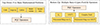 |
Figure 34. Top-down and bottom up reconfigurability |
(1) Top-down Reconfigurability. From a top-down perspective, agile PQC hardware must allow reconfiguration at the algorithmic, control, and communication layers. The architecture should consist of cryptographic compute clusters connected by a reconfigurable interconnect and controlled by a lightweight orchestration processor. These clusters can be reassigned to some PQC families: lattice (e.g., Kyber, SABER, Dilithium), code (e.g., BIKE, HQC), hash (e.g., Sphincs+), multivariate (e.g., Rainbow-like), or isogeny-based (e.g., SIDH/SIKE successors). This modular partitioning enables concurrent execution or pipelining of different algorithms, supporting hybrid PQC modes and multi-layered defense strategies. The support of these five basic PQC families can help the agile PQC platform be extended to other PQC schemes or future algorithms.
Moreover, the top-down design should integrate algorithm-level task abstraction. For example, generic primitives like randomness generation, matrix–vector multiplication, hash/Pseudo-Random Number Generator (PRNG), and NTT-transform can be encoded as specific tasks, later mapped to concrete hardware operators depending on the active PQC algorithm. The top-down agility thus bridges the algorithmic diversity of PQC with the physical constraints of silicon, ensuring the system can dynamically reorient its cryptographic posture as quantum threats evolve.
(2) Bottom-up Reconfigurability. At the bottom layer, reconfigurability stems from the ability of the arithmetic and logic units to natively support diverse algebraic structures. The arithmetic kernel should be designed to operate in prime fields 𝔽p, binary extension fields GF(2n), and polynomial rings ℤq[x]/(xn + 1). All of these structures underpin the basic structure of the mainstream PQC algorithms: lattice-based schemes rely on modular and ring-arithmetic; code-based cryptography depends on binary field operations; and isogeny-based and multivariate schemes involve large-integer modular or mixed-field operations.
To achieve operator versatility, arithmetic units must incorporate configurable modular multipliers, carry-save accumulators, polynomial multipliers, and butterfly computation engines, just as ref. [50]. By dynamically adjusting modulus parameters, coefficient width, and polynomial degrees, a single computational array can switch between NTT/INTT transforms, finite-field multiplications, and syndrome calculations. Shared multi-field operators can thus reduce silicon redundancy and enable runtime flexibility. Furthermore, the memory subsystem should provide a flexible access pattern to adapt to different PQC dataflows. Such bottom-up adaptability ensures that the arithmetic layer acts as a universal foundation for any PQC instantiation.
(3) Randomness Generation. Randomness plays a critical role in all PQC algorithms by providing entropy for key generation, noise sampling, and masking. In agile hardware, the randomness subsystem must be as flexible as the computation core itself. Two orthogonal types of randomness are required: location randomness and value randomness.
Location randomness governs the arrangement or order of data, controlling memory and computational flow. Examples include Fisher–Yates shuffling and constant-time sorting. Implementing Location randomness in hardware requires lightweight permutation networks or shuffle sorting engines that can reconfigure address mapping dynamically based on seeded randomness.
Value randomness, by contrast, deals with the statistical distribution of the numbers generated. It originates from high-entropy sources, such as true random number generators or cryptographically secure PRNGs. In PQC implementations, these values are essential for sampling uniform or binomial noise and generating ephemeral keys. An agile hardware design should incorporate a configurable randomness engine capable of tuning distribution parameters, entropy sources, and throughput. This flexibility guarantees that the randomness subsystem remains compatible with future PQC schemes that may require different sampling profiles or statistical guaranties.
In summary, an agile PQC hardware platform featuring pre-silicon static agility, bottom-up algebraic versatility, and top-down algorithmic reconfigurability offers a sustainable defense framework for the quantum era. By embedding universal algebraic operators, flexible task management, and reconfigurable randomness generation, the same silicon can securely accelerate algorithms across all major PQC families. This “multi-mathematical backup" approach transforms hardware from a fixed-purpose accelerator into an adaptive cryptographic fabric.
5.3.2. Post-silicon dynamic agility
While pre-silicon static agility guarantees multiple algorithmic compatibility at design time, true resilience in the quantum era requires post-silicon dynamic agility, which enables the deployed PQC hardware to adapt in real time after fabrication, especially when new cryptoanalysis attacks emerge. Once large-scale quantum computers become practical, certain mathematical assumptions, such as the hardness of lattice problems, may be severely weakened. In such a scenario, even standardized algorithms like Kyber or Dilithium could be rendered insecure. Hardware systems deployed across communication infrastructures, data centers, and embedded devices must therefore possess the capacity to transition to alternative PQC families instantly, without the need for costly hardware replacement or downtime.
Based on the stage of reconfiguration, the reconfiguration solutions can be divided into two methods: and Deployment-Time Reconfiguration and Run-Time Reconfiguration.
(1) Deployment-Time Reconfiguration. Post-silicon agility can be achieved through deployment-time reconfiguration, in which the PQC DSA dynamically modifies its configuration text, which reconfigures the computational pathways, arithmetic units, and memory access patterns based on secure software or firmware updates. Unlike static FPGA bitstream reconfiguration–which requires full or partial device reprogramming and may take seconds or even minutes–dynamic reconfiguration of PQC DSA [50, 51] is orchestrated through lightweight, data-driven control mechanisms embedded directly in the hardware datapath. This approach allows the device to switch between cryptographic algorithms or parameter sets in microseconds, achieving an improvement of up to four orders of magnitude in reconfiguration latency compared to traditional FPGA-level updates.
(2) Run-Time Reconfiguration. The cornerstone of run-Time Reconfiguration is data-packet-based reconfiguration. Instead of reloading new configuration files, the hardware adapts its operation according to the structure and semantics of the incoming data packets. The new data packet carries meta-information–such as operation type, field modulus, key size, or polynomial length–that guides the internal configuration of computational units on the fly.
This data-driven paradigm enables continuous operation without stopping or resetting the whole chip. The reconfiguration occurs in line with normal data processing, ensuring that throughput remains uninterrupted while the hardware context self-adjusts to new PQC workloads. Furthermore, this fine-grained control allows distinct cryptographic domains to coexist concurrently in a heterogeneous compute fabric, facilitating hybrid encryption or migration scenarios where multiple PQC families are simultaneously employed for enhanced resilience. To realize such agility, the architecture of PQC DSA must embed reconfiguration controllers at the task-path and operator levels.
6. Future PQC hardware: insights and perspectives
The rapid evolution of PQC requires continuous innovation in hardware design to address emerging challenges such as quantum threats, algorithmic diversity, and energy constraints. In addition, there are also some remaining problems in the existing research. As the PQC standards are solidified and the deployment scales, future hardware must prioritize scalability, efficiency, and adaptability to support long-term security. This chapter explores the anticipated directions in PQC hardware, focusing on technological advancements, architectural changes, and ecosystem developments that will shape the next generation of quantum-resistant systems. Drawing from current research trends and implementation lessons, we analyze how innovations in design methodologies and defense strategies will enable more robust and agile PQC solutions. The discussion encompasses both near-term improvements and long-term visions, highlighting key areas like advanced agile crypto-hardware, migrateble PQC hardware, multiple defense strategy against SCA/FIA and cryptoanalysis-hardware optimization.
6.1. Agile PQC hardware and domain-specific support
Rapid advances in PQC DSA implementation [50, 173, 174], highlighted by high-performance designs reported in the proceedings of the ISSCC’24 [50], demonstrate that achieving low-latency, high-throughput PQC operation is feasible for the primary NIST standards. However, the next phase of research must move beyond optimizing individual or limited algorithms toward building resilient, adaptable architectures. This strategic shift on the server-side involves embracing agile PQC DSA-a hybrid hardware-software approach–as the fundamental building block for future cryptographic systems. The following subsections detail five critical research challenges and limitations that must be addressed to realize truly flexible, secure, and future-proof PQC hardware.
6.1.1. Enough algorithmic flexibility and the challenge of universal hardware
Despite significant progress in hardware design, current agile PQC DSA architectures exhibit limited flexibility, primarily unifying operations within the dominant lattice family (ML-KEM and ML-DSA). And state-of-the-art DSAs [31, 50] only support three types of mathematical problems. The ambition of a single, unified DSA capable of efficiently accelerating all five major PQC mathematical families (Lattice-Based, Code-Based, Hash-Based, Multivariate-Based and Isogeny-Based) remains an unfulfilled research goal.
The fundamental hurdle is the incompatibility of core arithmetic primitives. Lattice schemes rely on polynomial arithmetic and the NTT modules, demanding dedicated Polynomial Multipliers. In contrast, Isogeny-based schemes (e.g., SIKE, SQIsign) are constrained by long-integer modular arithmetic, requiring specialized Montgomery Multipliers and complex carry-handling logic. Code-based schemes (HQC, BIKE) rely on intricate finite-field operations (GF(2m)) and massive linear algebra (syndrome decoding/Gaussian elimination). Unifying all these demands into a single arithmetic unit would result in prohibitive area and power overhead due to the large number of disparate functional units, specialized routing, and control logic required to switch between different fields, such as GF(2m) XOR-based operations and long-integer carries. Future research must, therefore, focus on Modular Heterogeneity: designing DSA cores not as a single unified ALU, but as a cluster of reconfigurable PE array supporting multiple fields and rings managed by a unified scheduling layer, thereby optimizing resource allocation without sacrificing computational versatility.
6.1.2. The design of domain-specific PQC compilers
The rapid pace of PQC development is stifled by the pervasive lack of dedicated, domain-specific compilers capable of bridging the gap between high-level cryptographic algorithms and after-silicon support. Current PQC hardware flows are heavily based on manual RTL coding (a time-consuming process prone to implementation errors) or general-purpose HLS tools, which, while faster, often fail to exploit PQC-specific algebraic and parallelization opportunities.
The limitations imposed by this deficiency are severe.
- (1)
Manual Optimization Burden: Without domain-aware compilation, designers must manually decompose complex algebraic operations (like address mapping and sequence reordering) into low-level configuring context, hindering rapid architectural exploration and performance tuning (e.g., selecting optimal Karatsuba vs. Toom-Cook splits). Besides, the execution efficiency of automatic mapping needs to achieve 80% of manual optimization while the mapping speed accelerated by two or three magnitudes.
- (2)
Implementation Security Gaps: The absence of automated compiler checks increases the risk of introducing critical security flaws. A dedicated PQC compiler could integrate formal verification methods to automatically enforce constant-time execution and ensure the correct placement and utilization of masking shares across the datapath, a capability currently underdeveloped.
Conversely, the presence of a PQC Compiler Suite would offer several potential advantages: (1) Accelerated Design Space Exploration: automation tools could be integrated to automatically explore the massive architectural space, optimizing for metrics like Time-Area Product based on high-level parameter changes. (2) Automated Code Generation: A compiler could generate optimized and parameterized hardware code for all security levels of a given PQC family from a single high-level description, significantly reducing the development cycle from years to months. (3) Security-Driven Mapping: Most importantly, it would enable security-driven mapping, where the compiler guarantees, via formal proof, that the security properties (such as constant-time) are preserved from the algorithm specification down to the final configuration context.
6.1.3. Break the throughput bottlenecks: achieving real-world signature rates
Although existing hardware research often cites excellent latency (time for a single operation), achieving the high operational throughput required for modern network infrastructure remains a significant challenge, particularly for DS. Current implementations, even highly optimized ones, often fall short of industrial demands. Although some KEM decapsulation times are fast enough to achieve well over 100 000 ops/s (e.g., certain Kyber decapsulation implementations [50]), signature generation rates struggle. The need for real-world DSA operation rates is often cited at 50 000 ops/s or higher, yet many robust implementations, especially for Sphincs+, deliver significantly lower rates due to their sequential nature, with some robust versions achieving closer to 1000 ops/s.
The path to achieving 50 000 ops/s [173] or more requires hardware research to transition from single-task optimization to high-concurrency pipeline design. For lattice-based DSAs like Dilithium and Falcon, this means accelerating the computationally heavy final stages, such as coefficient compression and encoding/decoding, which often become the new critical path after core arithmetic (NTT) is solved. For Sphincs+, the research must innovate methods for introducing parallelism into the inherently sequential WOTS+ chain and MT traversal, potentially via massive multi-core parallel hash function execution and advanced scheduling to minimize data dependencies.
6.1.4. Seamless co-migration: integrating PQC with classical public key cryptography
A major limitation of current PQC hardware is its incompatibility with established traditional PKC schemes, such as RSA and ECC. This exclusion forces systems to undertake a high-risk, “rip-and-replace” transition rather than a phased, hybrid co-migration. During the uncertain period of PQC standardization and deployment, the most secure approach for many organizations (including government agencies) is to use a hybrid KeyShare protocol (e.g., Kyber + Elliptic Curve Diffie–Hellman (ECDH)) to combine the security confidence of classical algorithms with the quantum resistance of the new schemes.
Current PQC DSA architectures are ill-suited for this hybrid requirement because the core arithmetic primitives are fundamentally different: ECC/RSA rely on long-integer Montgomery multipliers for modular exponentiation, while ML-KEM/ML-DSA rely on NTT-based arithmetic. Future migratable PQC hardware must integrate a dual-mode ALU capable of efficiently executing both sets of operations, with hundreds of thousands of OPS throughput in traditional public-key schemes. Research must focus on design methodologies that allow seamless, low-latency switching between different modes of algorithms, enabling a single DSA to serve as the unified accelerator for hybrid protocols. Such co-optimization is the key to creating practical, risk-mitigated cryptographic solutions for long-lived systems.
6.1.5. Agile defense: agile hardware and side-channel resistance
The agile defense paradigm represents the strategic need to leverage flexible PQC hardware architectures to dynamically enforce robust resistance against physical attacks, specifically SCA. Although conventional designs rely on static hardwired countermeasures, the agility inherent in DSA can be utilized to implement dynamic obfuscation techniques such as flexible masking, execution randomization (shuffling), and redundancy. This is crucial for lattice-based schemes like Kyber and Dilithium, where the DSA architecture facilitates a masked design; custom tasks are invoked to securely delegate sensitive operations, like the NTT, ensuring that masking shares are managed safely and efficiently across the datapath. Furthermore, the core flexibility of the PQC control unit enables architectural defenses that employ temporal randomization: a sophisticated scheduler can implement out-of-order execution or redundant execution checks to deliberately decorrelate power traces, preventing statistical analysis (DPA and Correlation Power Attack, CPA) that relies on fixed timing patterns. Advanced techniques, such as higher-order time sharing masking, leverage hardware properties to achieve glitch-included security, demonstrating continuous evolution in flexible, low-latency protection. For FIA, this agility is manifest in full hardware duplication–a robust countermeasure against clock and voltage glitches demonstrated for Sphincs+–where the DSA’s ability to manage two parallel processing cores simultaneously provides fault detection at the system level. By embedding these dynamic, randomized, and verifiable countermeasures directly into the execution flow, agile hardware transcends mere cryptographic flexibility to provide a necessary layer of security agility against an ever-evolving landscape of classical adversaries.
Besides the points mentioned above, in the pursuit of efficient PQC hardware, Processing-in-Memory (PIM) architectures have already been successfully adopted in recent literature. These works demonstrate that PIM can effectively alleviate the memory-bound bottlenecks inherent in lattice-based schemes. However, the application of advanced packaging technologies–specifically 3D stacking and chiplets–to PQC remains unexplored, with no silicon-verified implementations currently reported. Looking ahead, we anticipate a divergence in the adoption of these technologies. Chiplet-based design is poised to become a promising future direction, offering a modular approach to integrate heterogeneous PQC accelerators with general-purpose processors. However, 3D vertical stacking is unlikely to see immediate adoption in this domain, as the current bandwidth requirements of PQC standards may not yet justify the high manufacturing costs and thermal design complexities associated with 3D integration.
6.2. SCA and FIA resistant PQC hardware
6.2.1. Current status of SCA/FIA resistant PQC hardware
The development of resistant PQC hardware is guided by the imperative that mathematical security (quantum resistance) must be complemented by physical security. Research efforts have yielded significant processes in hardening PQC implementations against passive SCA and active FIA. The current physical security state of PQC, which includes the five main algorithmic families, is summarized in Table 8. The work [175] proposed a novel ShiftMod masking gadgets for efficient arithmetic shifts and new Boolean-to-arithmetic conversion scheme to support masked PQC. The work [176] masked the software implementation of Kyber on Cortex-M4 and achieved the first fully-masked implementation. Fritzmann et al. [177] utilized a masked HW/SW co design with a novel masked ciphertext compression algorithm for any moduli. ElGhamrawy et al. [52] constructed a differential fault attack on the randomized and deterministic versions of Dilithium and then proposed the algorithmic countermeasures. Tian et al. [33] masked Gauss-elimination process to protect code-based/multivariate-based PQC. Norga et al. [178] implemented a code-based ISE to mask code-based PQC based on a RISC-V unit. The masking and FIA detection strategies of multivariate, isogeny-based PQC implementations lack deep researches because of the ongoing standardization process. Future researches can be explored with the continuous standardization of different institutes and wide-application.
Existing FIA/SCA-resistant PQC solutions
6.2.2. Future SCA/FIA resistant PQC hardware
Future research must focus on closing the remaining security gaps, ensuring that all PQC families possess robust, verifiable countermeasures in both hardware and software, especially considering the constraints of Agile DSA designs.
The research roadmap can be defined by the following strategic needs.
- (1)
Closing the Isogeny and Hash Software Gaps: The most prominent software deficiency is the lack of public implementations for Isogeny-Based and Hash-Based masking. For Isogeny schemes, this requires developing masked long-integer arithmetic libraries suitable for execution on host processors, which is critical for supporting hybrid systems. For Hash-Based schemes, the complexity lies in masking the large number of sequential hash calls or the MT traversal structure, demanding research into structurally-aware masking schedulers that randomly interleave or redundantly execute hash operations in software to prevent statistical analysis.
- (2)
Formalizing FIA Detection for Multivariate and Hash Schemes: Both Multivariate (Rainbow) and Hash-Based schemes currently lack published, formalized efficient algorithmic fault detection methods in both hardware and software; current defense against FIA is largely confined to the expensive countermeasure of full hardware duplication. Future work must address this by developing redundant checks specific to the linear algebra of multivariate schemes and the hash-chain properties of hash-based schemes. For Multivariate schemes, this involves embedding checks within the parallel processing element array that verifies the algebraic consistency of the Gaussian elimination steps.
- (3)
Cross-Domain Resilient DSAs/ISE: Future Agile PQC DSAs must integrate the best-in-class security features to achieve true resilience. This involves designing leak-resistant instruction set architectures where custom instructions are intrinsically masked and timed independently of data, thereby ensuring that the flexibility of the DSA does not create new side-channel paths. This requires the security engine to intelligently manage masking shares and constant-time execution across wildly different hardware domains, including the NTT units (lattice), GF(2m) processors (code/multivariate) and long-integer ALUs (isogeny), all from a single complete security specification. This holistic approach is essential to formalize the security boundaries of agile PQC hardware.
6.3. PQC Cryptoanalysis-ASIC co-optimization
The successful future of PQC hardware development is also related to algorithmic cryptanalysis and parameter tuning, a principle best exemplified by the work of Kundu et al. [180]. This research demonstrates the critical trend of PQC Cryptoanalysis-ASIC Co-Optimization by deliberately adjusting parameters of the Module-LWE problem–the mathematical foundation for Kyber to achieve silicon-level superiority. The core approach involved a scrupulous analysis of the design space, evaluating how factors such as polynomial size, field modulus structure, and the reduction algorithm impacted physical metrics. By tuning these elements based on hardware cost rather than purely mathematical security margins, the implementation of ASIC achieved remarkable efficiency: it delivered a 3× reduction in the area footprint compared to previous state-of-the-art Kyber designs and resulted in a 2× improvement in the crucial time-area product metric for its multiplication unit. This work fundamentally proves that for resource-constrained environments, achieving the optimal PQC solution requires hardware constraints to inform the initial design and parameter selection of the cryptographic scheme itself, establishing a new requirement for ASIC design to engage directly with cryptographic parameter optimization.
This critical need for PQC cryptoanalysis-ASIC co-optimization must be expanded across all PQC families to unlock the next generation of secure hardware. For Code-Based Cryptography (HQC, BIKE), future research must involve cryptanalysis-informed hardware design where the code’s structural parameters (e.g., Goppa code degree, quasi-cyclic block length) are adjusted based on the resource consumption and performance variability of the dedicated syndrome decoding hardware.
For hash-Based Signatures (SLH-DSA/Sphincs+), the co-optimization lies in tuning the WOTS+ and FORS parameters based on the number of available parallel hash accelerator units, thereby balancing signature size against the speed of sequential hash chain operations. Similarly, Multivariate-Based schemes (e.g., Rainbow) require that the complexity of the core algebraic system solver (e.g., the 2D PE array used for Gaussian elimination) be factored into the choice of the finite field and the number of variables to ensure the complex elimination process is performed efficiently in a constant-time manner, resisting SCA. Ultimately, this convergence demands a formal methodology in which cryptographic security proofs are continuously checked against, and informed by, the physical constraints and vulnerability profiles introduced at the RTL and silicon level, solidifying the trend of making hardware architects and cryptographers joint stakeholders in the final security posture of a PQC system.
7. Conclusion
The transition to a PQC landscape is not a distant, theoretical exercise but a pressing, practical imperative. This review has shown that PQC chips–specialized hardware solutions designed to protect the digital infrastructure against the threat of large-scale quantum computers–are the cornerstone of this cryptographic evolution. Their development and deployment are driven by the undeniable reality of the “Harvest Now, Decrypt Later" threat, a scenario in which sensitive data encrypted with today’s vulnerable algorithms are stored for future decryption by a quantum adversary. Our analysis reveals that while the software ecosystem is making strides, the full promise of PQC–especially in terms of performance, energy efficiency, and robust physical security–can only be realized through purpose-built hardware.
The core implementation challenge confronting PQC chip architects, as analyzed in the Section 2, stems from the profound diversity of quantum-resistant algorithms. This inherent heterogeneity invalidates any singular monolithic design approach, which requires highly specialized processing capabilities unique to all cryptographic families. Lattice-based schemes (Kyber, Dilithium) are critically bottlenecked by NTT and Polynomial Arithmetic, requiring specialized NTT engines or Karatsuba hardware to handle high-degree polynomial multiplication. This contrasts sharply with code-based schemes (McEliece, HQC, BIKE), which face multiple challenges of managing massive high storage pressure from multi-megabyte keys, alongside implementing complex, time-consuming algebraic decoders like the Syndrome Decoding (McEliece, HQC) or iterative Bit-Flipping (BIKE) decoders. Hash-based signatures (Sphincs+) face a unique challenge in minimizing latency caused by millions of sequential hash function calls, requiring Parallel Hash Accelerator designs to maximize throughput through highly-parallel hash accelerator. Finally, Isogeny-based schemes (SQIsign) are limited by long-integer modular reduction, demanding dedicated multi-precision Montgomery multiplication units.
Successful PQC deployment is necessarily platform-agnostic, spanning general-purpose processors augmented with ISE, flexible FPGA Accelerators for rapid prototyping, and highly optimized ASICs for achieving maximum performance and power efficiency in mass-market deployment. However, the strategic answer to the fluid standardization landscape of PQC algorithms may lie in an agile PQC DSA that balances performance and flexibility. It can rapidly change the portfolio of viable algorithms if there are new cryptanalytic attacks. This advanced design paradigm, detailed in Section 3, moves beyond static hardware by embracing hardware-software co-design. This methodology ensures that the software layer maintains control and adaptability, while the dedicated hardware core provides ASIC-like speed for computationally intensive primitives (e.g., NTT engines). This unified, flexible approach ensures the crucial crypto-agility required to support multiple algorithmic families (ML-KEM, ML-DSA) and to seamlessly update protocols and parameters in the field, guaranteeing that the system is future-proof against cryptographic uncertainties.
Looking ahead, the direction of PQC hardware research must focus on the full integration across all deployment scales. Future work must prioritize the development of migratable PQC Hardware for high-throughput server environments, capable of dynamically scaling and updating protocols to meet evolving standards. Concurrently, the focus on endpoint security must intensify, demanding the creation of SCA-resistant Hardware and FIA-resistant hardware to mitigate physical threats documented against core schemes like Kyber and Dilithium. This requires the integration of sophisticated defenses: higher-order masking against power analysis and algorithmic checks paired with physical primitives like Physically Unclonable Functions (PUFs) and True-Random Number Generators (TRNGs) for fault and key-leakage protection. Ultimately, the emerging field of PQC Cryptoanalysis-ASIC Co-Optimization underscores the necessity for continuous, iterative collaboration between cryptanalysts and silicon designers, ensuring the final deployed system is robust against both quantum and classical physical adversaries throughout the device’s entire lifecycle.
Funding
This work was supported by the National Key R&D Program of China (Grant Nos. 2023YFB4403500, 2024YFB3108103), the National Natural Science Foundation of China (Grant Nos. 62274102, 62504134), the fellowship of China National Postdoctoral Program for Innovative Talents (Grant No. BX20240204), the fellowship from the China Postdoctoral Science Foundation (Grant No. 2025M780516).
Conflicts of interest
The authors declare no conflicts of interest.
Data availability statement
No data are associated with this article.
Author contribution statement
Yihong Zhu carried out the layout of this survey; Yihong Zhu and Leibo Liu conducted detailed research and wrote this survey.
Acknowledgments
No acknowledgments.
References
- Kim Y, Eddins A, Anand S, et al. Evidence for the utility of quantum computin before fault tolerance. Nature 2023; 618: 500–505. [Google Scholar]
- Kam JF, Kang H, Hill CD, et al. Characterization of entanglement on superconducting quantum computers of up to 414 qubits. Phys Rev Res 2024; 6: 033155. [Google Scholar]
- Rivest RL, Shamir A and Adleman L. A method for obtaining digital signatures and public-key cryptosystems. Commun ACM 1978; 21: 120–126. [CrossRef] [Google Scholar]
- Rahman H and Azad S. Elliptic curve cryptography. Pract Cryptogr 2014; 147. https://csrc.nist.gov/Projects/Elliptic-Curve-Cryptography. [Google Scholar]
- Shor PW. Algorithms for quantum computation: Discrete logarithms and factoring. In: Proceedings 35th Annual Symposium on Foundations of Computer Science, 1994, 124–134. [Google Scholar]
- Mascelli J and Rodden M. Harvest now decrypt later: Examining post-quantum cryptography and the data privacy risks for distributed ledger networks. Financ Econ Discuss Ser 2025-09, 2025. https://doi.org/10.17016/FEDS.2025.093. [Google Scholar]
- Regev, O. (2024). On Lattices, Learning with Errors, Random Linear Codes, and Cryptography. https://arxiv.org/abs/2401.03703. [Google Scholar]
- Banerjee A, Peikert C and Rosen A. Pseudorandom functions and lattices. In: Advances in Cryptology – EUROCRYPT 2012. Berlin, Heidelberg: Springer, 2012, 719–737. [Google Scholar]
- Alekhnovich M. More on average case vs. approximation complexity. IEEE, 2003, 298–307. [Google Scholar]
- Ajtai M. Generating hard instances of lattice problems (extended abstract). In: Proceedings of the Twenty-Eighth Annual ACM Symposium on Theory of Computing, STOC ’96. New York, NY, USA: Association for Computing Machinery, 1996, 99–108. [Google Scholar]
- Boudgoust K, Jeudy C, Roux-Langlois A, et al. Towards classical hardness of module-LWE: The linear rank case. In Advances in Cryptology – ASIACRYPT 2020. Cham: Springer International Publishing, 2020, 289–317. [Google Scholar]
- Lyubashevsky V, Peikert C and Regev O. On ideal lattices and learning with errors over rings. In: Gilbert H, editor, Advances in Cryptology – EUROCRYPT 2010. Berlin, Heidelberg: Springer, 2010, 1–23. [Google Scholar]
- Alagic G, Cooper D, Dang Q, et al. Status report on the third round of the NIST post-quantum cryptography standardization process, 2022. [Google Scholar]
- Avanzi R, Bos J, Ducas L, et al. CRYSTALS-Kyber algorithm specifications and supporting documentation (version 3.02). US Department of Commerce, NIST, 2017. [Google Scholar]
- Bai S, Ducas L, Kiltz E, et al. CRYSTALS-Dilithium algorithm specifications and supporting documentation (Version 3.1). US Department of Commerce, NIST, 2021. [Google Scholar]
- Weger V, Gassner N and Rosenthal J. A survey on code-based cryptography. arXiv preprint arXiv: https://arxiv.org/abs/2201.07119, 2022. [Google Scholar]
- Aumasson J-P, Bernstein DJ, Beullens W, et al. SPHINCS+ submission to the NIST post-quantum project, v.3. US Department of Commerce, NIST, 2020. [Google Scholar]
- Joseph D, Misoczki R, Manzano M, et al. Transitioning organizations to post-quantum cryptography. Nature 2022; 605: 237–243. [Google Scholar]
- Vermeer MJD and Peet ED. Securing Communications in the Quantum Computing Age: Managing the Risks to Encryption. Santa Monica, CA: RAND Corporation, 2020. [Google Scholar]
- Alagic G, Alperin-Sheriff J and Apon D. Status report on the first round of the NIST post-quantum cryptography standardization process, 2019. [Google Scholar]
- Fouque P-A, Hoffstein J, Kirchner P, et al. Falcon: Fast-Fourier lattice-based compact signatures over NTRU specification v1.2 – 01/10/2020. US Department of Commerce, NIST, 2020. [Google Scholar]
- National Institute of Standards and Technology (NIST). FIPS 203: Module-lattice-based key-encapsulation mechanism standard. U.S. Department of Commerce, 2024. https://csrc.nist.gov/pubs/fips/203/final. [Google Scholar]
- National Institute of Standards and Technology (NIST). FIPS 204: Module-lattice-based digital signature standard. U.S. Department of Commerce, 2024. https://csrc.nist.gov/pubs/fips/204/final. [Google Scholar]
- National Institute of Standards and Technology (NIST). FIPS 205: Stateless hash-based digital signature standard. U.S. Department of Commerce, 2024. https://csrc.nist.gov/pubs/fips/205/final. [Google Scholar]
- Melchor CA, Aragon N, Bettaieb S, et al. Hamming Quasi-Cyclic (HQC) fourth round version. US Department of Commerce, NIST, 2024. [Google Scholar]
- ISO/IEC. Information security – Digital signatures with appendix – Part 4: Stateful hash-based mechanisms: ISO/IEC FDIS 14888-4. International Organization for Standardization, 2023. https://www.iso.org/standard/80492.html. [Google Scholar]
- Buchmann J, Dahmen E and Hülsing A. XMSS-a practical forward secure signature scheme based on minimal security assumptions. Springer, 2011, 117–129. [Google Scholar]
- Cooper D, Apon D, Dang Q, et al. Recommendation for stateful hash-based signature schemes: 800-208. National Institute of Standards and Technology, 2020. [Google Scholar]
- Bernstein DJ, Chou T, Cid C, et al. Classic McEliece: Conservative code-based cryptography cryptosystem specification. US Department of Commerce, NIST, 2022. https://classic.mceliece.org/nist/mceliece-20201010.Pdf. [Google Scholar]
- Bos J, Costello C, Ducas L, et al. Frodo: Take off the ring! Practical, Quantum-Secure Key Exchange from LWE[EB/OL]. Cryptology ePrint Archive, Paper 2016/659, 2016. https://doi.org/10.1145/2976749.2978425. [Google Scholar]
- Zhu Y, Zhu W, Li C, et al. RePQC: A 3.4-μJ/Op 48-kOPS post-quantum crypto-processor for multiple-mathematical problems. IEEE J Solid-State Circuits 2022; 58: 124–140. [Google Scholar]
- Schöffel M, Feldmann J, Wehn N. Code-based Cryptography in IoT: A HW/SW Co-Design of HQC, in: 2022 IEEE 8th World Forum on Internet of Things (WF-IoT), Yokohama, Japan, 2022, pp. 1–7, https://doi.org/10.1109/WF-IoT54382.2022.10152031. [Google Scholar]
- Tian Q, Cheng H, Guo C, et al. A code-based ISE to protect Boolean masking in software. IACR Trans Cryptogr Hardw Embed Syst, 2025. [Google Scholar]
- Wang T, Zhang C, Zhang X, et al. Optimized hardware-software co-design for Kyber and Dilithium on RISC-V SoC FPGA. IACR Trans Cryptogr Hardw Embed Syst 2024; 2024: 99–135. [Google Scholar]
- Abdulrahman A, Kannwischer MJ and Lim T-H. Enabling microarchitectural agility: Taking ML-KEM & ML-DSA from Cortex-M4 to M7 with SLOTHY. In: ACM AsiaCCS 2025, 2025. [Google Scholar]
- Mera JMB, Turan F, Karmakar A, et al. Compact domain-specific co-processor for accelerating module lattice-based KEM. In: 2020 57th ACM/IEEE Design Automation Conference (DAC), 2020, 1–6. [Google Scholar]
- Wang W, Szefer J and Niederhagen R. Solving large systems of linear equations over GF(2) on FPGAs. In: 2016 International Conference on ReConFigurable Computing and FPGAs (ReConFig), 2016, 1–7. [Google Scholar]
- Chen P-J, Chou T, Deshpande S, et al. Complete and improved FPGA implementation of classic McEliece. Cryptology ePrint Arch 2022. [Google Scholar]
- Roy SS, Vercauteren F, Mentens N, et al. Compact Ring-LWE cryptoprocessor. In: Batina L and Robshaw M, editors, Cryptographic Hardware and Embedded Systems – CHES 2014. Berlin, Heidelberg: Springer, 2014, 371–391. [Google Scholar]
- Howe J, Oder T, Krausz M, et al. Standard lattice-based key encapsulation on embedded devices. IACR Trans Cryptogr Hardw Embed Syst 2018; 2018: 372–393. [Google Scholar]
- Du C and Bai G. Towards efficient polynomial multiplication for lattice-based cryptography. In: 2016 IEEE International Symposium on Circuits and Systems (ISCAS), 2016, 1178–1181. [Google Scholar]
- Fritzmann T, Sharif U, Müller-Gritschneder D, et al. Towards reliable and secure post-quantum co-processors based on RISC-V. In: 2019 Design, Automation Test in Europe Conference Exhibition (DATE), 2019, 1148–1153. [Google Scholar]
- Song S, Tang W, Chen T, et al. LEIA: A 2.05 mm2 140mW lattice encryption instruction accelerator in 40nm CMOS. In: 2018 IEEE Custom Integrated Circuits Conference (CICC). IEEE, 2018, 1–4. [Google Scholar]
- Banerjee U, Juvekar C, Wright A, et al. An energy-efficient reconfigurable DTLS cryptographic engine for end-to-end security in IoT applications. In: 2018 IEEE International Solid-State Circuits Conference-(ISSCC). IEEE, 2018, 42–44. [Google Scholar]
- Hutter M, Schilling J, Schwabe P, et al. NaCl’s crypto box in hardware, 2016. [Google Scholar]
- Basu K, Soni D, Nabeel M, et al. NIST post-quantum cryptography-A hardware evaluation study. IACR Cryptol ePrint Arch 2019; 2019: 47. [Google Scholar]
- Fritzmann T and Sepúlveda J. Efficient and flexible low-power NTT for lattice-based cryptography. In: 2019 IEEE International Symposium on Hardware Oriented Security and Trust (HOST), 2019. [Google Scholar]
- Nejatollahi H, Dutt ND, Banerjee I, et al. Domain-specific accelerators for ideal lattice-based public key protocols. IACR Cryptol ePrint Arch 2018; 2018: 608. [Google Scholar]
- Farahmand F. Implementing and benchmarking seven Round 2 lattice-based key encapsulation mechanisms using a software/hardware codesign approach, 2019. [Google Scholar]
- Zhu Y, Zhu W, Ouyang Y, et al. A 28nm 69.4kOPS 4.4μJ/Op versatile post-quantum crypto-processor across multiple mathematical problems. In: 2024 IEEE International Solid-State Circuits Conference (ISSCC), Vol. 67, 2024, 298–300. [Google Scholar]
- Zhu Y, Zhu W, Ouyang Y, et al. PQPU: A 4.4-μJ/Op 69.4-kOPS agile post-quantum crypto-processor across multiple mathematical problems. IEEE J Solid-State Circuits 2025; 60: 2261–2275. [Google Scholar]
- ElGhamrawy M, Azouaoui M, Bronchain O, et al. From MLWE to RLWE: A differential fault attack on randomized & deterministic dilithium. IACR Trans Cryptogr Hardw Embed Syst 2023; 2023: 565–594. [Google Scholar]
- Berzati A, Calle Viera A, Chartouny M, et al. Exploiting Intermediate Value Leakage in Dilithium: A Template-Based Approach[EB/OL]. Cryptology ePrint Archive, Paper 2023/050, 2023. https://eprint.iacr.org/2023/050. [Google Scholar]
- Dong H and Guo Q. Multi-value plaintext-checking and full-decryption oracle-based attacks on HQC from offline templates. IACR Trans Cryptogr Hardw Embed Syst 2025. https://ches.iacr.org/2025/acceptedpapers.php. [Google Scholar]
- Uhle F, Müller N and Moradi A. Fault injection evaluation with statistical analysis – How to deal with nearly fabricated large circuits. IACR Trans Cryptogr Hardw Embed Syst, 2025. https://ches.iacr.org/2025/acceptedpapers.php. [Google Scholar]
- D’Anvers J-P, Karmakar A, Roy SS, et al. Saber: Module-LWR based key exchange, CPA-secure encryption and CCA-secure KEM. In: Progress in Cryptology – AFRICACRYPT 2018. Springer, 2018, 282–305. [Google Scholar]
- D’Anvers J-P, Vercauteren F and Verbauwhede I. The impact of error dependencies on Ring/Mod-LWE/LWR based schemes. IACR Cryptol ePrint Arch 2018, Report 2018/1172. [Google Scholar]
- McEliece RJ. A public-key cryptosystem based on algebraic coding theory. Deep Space Netw Prog Rep 1978; 44: 114–116. [Google Scholar]
- Aragon N. BIKE:BIKE_Spec. US Department of Commerce, NIST, 2022. https://bikesuite.org/ [Google Scholar]
- Merkle RC. A digital signature based on a conventional encryption function. In: Advances in Cryptology – CRYPTO ’87. Lecture Notes in Computer Science, Vol. 293. Springer, 1987, 369–378. [Google Scholar]
- Huelsing A, Butin D, Gazdag S, et al. XMSS: EXtended Merkle signature scheme. RFC Editor, 2018. [Google Scholar]
- Liu G, Liu G, Jiang K, et al. Improving MPCitH with preprocessing: Mask is all you need. IACR Trans Cryptogr Hardw Embed Syst, 2025. https://ches.iacr.org/2025/acceptedpapers.php. [Google Scholar]
- Chen M-S, Petzoldt A, Schmidt D, et al. Rainbow-Round 2. US Department of Commerce, NIST, 2019. https://csrc.nist.gov/CSRC/media/Presentations/rainbow-round-2-presentation/images-media/rainbow-ding.pdf [Google Scholar]
- Ding J and Schmidt D. Rainbow, a new multivariable polynomial signature scheme. In: Applied Cryptography and Network Security (ACNS 2005). Lecture Notes in Computer Science, Vol. 3531. Springer, 2005, 164–175. [Google Scholar]
- Kipnis A, Patarin J and Goubin L. Unbalanced oil and vinegar signature schemes. In: Advances in Cryptology – EUROCRYPT ’99. Lecture Notes in Computer Science, Vol. 1592. Springer, 1999, 206–222. [Google Scholar]
- Jao D and De Feo L. Towards quantum-resistant cryptosystems from supersingular elliptic curve isogenies. In: Proceedings of the 4th International Conference on Post-Quantum Cryptography (PQCrypto 2011). Springer, 2011, 19–34. [Google Scholar]
- Jao D, Azarderakhsh R, De Feo L, et al. Supersingular isogeny key encapsulation. In: Submission to the NIST Post-Quantum Cryptography Standardization Project, 2017. [Google Scholar]
- Jao D, Azarderakhsh R and Campagna M. SIKE: Supersingular isogeny key encapsulation Round 3. US Department of Commerce, NIST, 2020. https://csrc.nist.gov/csrc/media/Projects/post-quantum-cryptography/documents/round-4/submissions/SIKE-spec.pdf [Google Scholar]
- De Feo L, Kohel DR, Leroux A, et al. SQISign: Compact post-quantum signatures from quaternions and isogenies. In: Advances in Cryptology–ASIACRYPT 2020. Springer, 2020, 64–93. [Google Scholar]
- Castryck W and Decru T. An efficient key recovery attack on SIDH. In: Hazay C and Stam M, editors. Cham, 2023, 423–447. [Google Scholar]
- Castryck W, Lange T, Martindale C, et al. CSIDH: An efficient post-quantum commutative group action. In: Galbraith S and Peyrin T, editors, Advances in Cryptology – ASIACRYPT 2018. Cham: Springer International Publishing, 2018, 395–427. [Google Scholar]
- Bruun NM. Z-transform DFT filters and FFT’s. IEEE Trans Acoust Speech Signal Process 1978; 26: 56–63. [Google Scholar]
- Karatsuba, A.A., & Ofman, Y. Multiplication of Multidigit Numbers on Automata. Soviet physics. Doklady, 1963; 7: 595–596. [Google Scholar]
- Sikeridis D, Kampanakis P and Devetsikiotis M. Assessing the overhead of post-quantum cryptography in TLS 1.3 and SSH. In: Proceedings of the 16th International Conference on Emerging Networking EXperiments and Technologies (CoNEXT ’20). ACM, 2020, 149–156. [Google Scholar]
- Sikeridis D, Kampanakis P and Devetsikiotis M. Post-quantum authentication in TLS 1.3: A performance study. In: NDSS Symposium 2020, 2020. [Google Scholar]
- Kampanakis P and Childs-Klein W. The impact of data-heavy, post-quantum TLS 1.3 on the Time-To-Last-Byte of real-world connections. In: Workshop on Measurements, Attacks, and Defenses for the Web (MADWeb) 2024, 2024. [Google Scholar]
- Sosnowski M, Wiedner F, Hauser E, et al. The performance of post-quantum TLS 1.3. In: Companion of the 19th International Conference on Emerging Networking EXperiments and Technologies (CoNEXT Companion) 2023, 2023. [Google Scholar]
- Campbell D, Rafferty C, Khalid A, et al. Acceleration of post quantum digital signature scheme crystals-dilithium on reconfigurable hardware. In: 2022 32nd International Conference on Field-Programmable Logic and Applications (FPL), 2022, 462–463. [Google Scholar]
- Malal A. Designing efficient and flexible NTT accelerators, 2023. https://eprint.iacr.org/2023/1617. [Google Scholar]
- Longa, P., Naehrig, M. (2016). Speeding up the Number Theoretic Transform for Faster Ideal Lattice-Based Cryptography. In: Foresti, S., Persiano, G. (eds) Cryptology and Network Security. CANS 2016. Lecture Notes in Computer Science, vol 10052. Springer, Cham. https://doi.org/10.1007/978-3-319-48965-0_8. [Google Scholar]
- Maeder RE. Storage allocation for the Karatsuba integer multiplication algorithm. In: Miola A, editor, Design and Implementation of Symbolic Computation Systems. Berlin, Heidelberg: Springer, 1993, 59–65. [Google Scholar]
- Wu Y, Bai G and Wu X. A Karatsuba algorithm based accelerator for pairing computation. In: 2019 IEEE International Conference on Electron Devices and Solid-State Circuits (EDSSC), 2019, 1–3. [Google Scholar]
- Pöppelmann T, Oder T, Güneysu T. High-performance ideal lattice-based cryptography on 8-Bit ATxmega microcontrollers. In: Lauter K and Rodríguez-Henríquez F, editors, Progress in Cryptology – LATINCRYPT 2015. Cham: Springer International Publishing, 2015, 346–365. [Google Scholar]
- Zhang N, Yang B, Chen C, et al. Highly efficient architecture of NewHope-NIST on FPGA using low-complexity NTT/INTT. IACR Trans Cryptogr Hardw Embed Syst 2020; 2020: 49–72. [Google Scholar]
- Zhu Y, Zhu W, Zhu M, et al. A 28nm 48KOPS 3.4μJ/Op agile crypto-processor for post-quantum cryptography on multi-mathematical problems. In: 2022 IEEE International Solid-State Circuits Conference (ISSCC), Vol. 65, 2022, 514–516. [Google Scholar]
- Li A, Lu J, Liu D, et al. A 40nm 2.76 μ J/O p energy-efficient secure post-quantum crypto-processor for Crystals-Kyber on module-LWE. In: 2023 IEEE Asian Solid-State Circuits Conference (A-SSCC), 2023, 1–3. [Google Scholar]
- Jung H, Dang Truong Q and Lee H. Highly-efficient hardware architecture for ML-KEM PQC standard. IEEE Open J Circuits Syst 2025; 6: 356–369. [Google Scholar]
- Zhu Y, Wang H, Zhu W, et al. High-speed hardware implementation of NTT/INTT-optimized LAC cryptosystem. Microelectron Comput 2025; 42: 187–195. [Google Scholar]
- Banerjee U, Pathak A and Chandrakasan AP. 2.3 an energy-efficient configurable lattice cryptography processor for the quantum-secure Internet of Things. In: 2019 IEEE International Solid-State Circuits Conference – (ISSCC), 2019, 46–48. [Google Scholar]
- Xin G, Han J, Yin T, et al. VPQC: A domain-specific vector processor for post-quantum cryptography based on RISC-V architecture. IEEE Trans Circuits Syst I: Regul Pap 2020; 67: 2672–2684. [Google Scholar]
- Zhao C, Zhang N, Wang H, et al. A compact and high-performance hardware architecture for CRYSTALS-Dilithium. IACR Trans Cryptogr Hardw Embed Syst 2021; 2022: 270–295. [Google Scholar]
- Ouyang Y, Zhu Y, Zhu W, et al. FalconSign: An efficient and high-throughput hardware architecture for Falcon signature generation. IACR Trans Cryptogr Hardw Embed Syst 2024; 2025: 203–226. [Google Scholar]
- Banerjee U, Ukyab TS and Chandrakasan AP. Sapphire: A configurable crypto-processor for post-quantum lattice-based protocols. IACR Trans Cryptogr Hardw Embed Syst 2019; 2019: 17–61. [Google Scholar]
- Zhu Y, Zhu M, Yang B, et al. LWRpro: An energy-efficient configurable crypto-processor for module-LWR. IEEE Trans Circuits Syst I: Regul Pap 2021; 68: 1146–1159. [Google Scholar]
- Hülsing A, Rijneveld J, Schanck J, et al. High-speed key encapsulation from NTRU. In: Fischer W and Homma N, editors. Cham: Springer International Publishing, 2017, 232–252. [Google Scholar]
- Ghosh A, Mera JMB, Karmakar A, et al. A 334 μW 0.158 mm2 ASIC for post-quantum key-encapsulation mechanism Saber with low-latency striding Toom–Cook multiplication. IEEE J Solid-State Circuits 2023; 58: 2383–2398. [Google Scholar]
- Wong Z-Y, Wong DC-K, Lee W-K, et al. KaratSaber: New speed records for Saber polynomial multiplication using efficient Karatsuba FPGA architecture. IEEE Trans Comput 2023; 72: 1830–1842. [Google Scholar]
- Deshpande S, Xu C, Nawan M, et al. Fast and efficient hardware implementation of HQC, 2022. https://eprint.iacr.org/2022/1183. [Google Scholar]
- Antognazza F, Barenghi A and Pelosi G. An efficient and unified RTL accelerator design for HQC-128, HQC-192, and HQC-256. IEEE Trans Comput 2025. [Google Scholar]
- Ras A, Loiseau A, Carmona M, et al. PHOENIX: Crypto-agile hardware sharing for ML-KEM and HQC. In: SecuElec Seminar/Cryptology ePrint Archive (presented May 2025), 2025. [Google Scholar]
- Antognazza F, Barenghi A, Pelosi G, et al. A high efficiency hardware design for the post-quantum KEM HQC. In: IEEE Symposium on Hardware Oriented Security and Trust (HOST) 2024, 2024. [Google Scholar]
- Antognazza F, Barenghi A, Pelosi G, et al. A versatile and unified HQC hardware accelerator. In: Applied Cryptography and Network Security Workshops (ACNS Workshops).Lecture Notes in Computer Science, Vol. 14587. Springer, 2024, 214–219. [Google Scholar]
- Galimberti A, Goli A, Sforza M, et al. FPGA-based design and implementation of a code-based post-quantum KEM. In: Applied Cryptography and Network Security Workshops (ACNS Workshops). Lecture Notes in Computer Science, Vol. 14587. Springer, 2024, 38–46. [Google Scholar]
- Reinders A H, Misoczki R, Ghosh S, et al. Efficient BIKE Hardware Design with Constant-Time Decoder[C]//2020 IEEE International Conference on Quantum Computing and Engineering (QCE). [S.l.]: IEEE, 2020: 197–204. https://doi.org/10.1109/QCE49297.2020.00033. [Google Scholar]
- Montanaro G., Galimberti A., Colizzi E. and Zoni D., “Hardware-Software Co-Design of BIKE with HLS-Generated Accelerators,” 2022 29th IEEE International Conference on Electronics, Circuits and Systems (ICECS), Glasgow, United Kingdom, 2022, pp. 1–4, https://doi.org/10.1109/ICECS202256217.2022.9970992 [Google Scholar]
- Bernstein DJ, Chou T and Schwabe P. McBits: Fast constant-time code-based cryptography. In: Bertoni G and Coron J-S, editors, Cryptographic Hardware and Embedded Systems – CHES 2013. Berlin, Heidelberg: Springer, 2013, 250–272. [Google Scholar]
- Chou T. Mcbits revisited. In: Fischer W and Homma N, editors, Cryptographic Hardware and Embedded Systems – CHES 2017. Cham: Springer International Publishing, 2017, 213–231. [Google Scholar]
- Dang VB, Mohajerani K and Gaj K. High-speed hardware architectures and FPGA benchmarking of CRYSTALS-Kyber, NTRU, and Saber. IEEE Trans Comput 2023; 72: 306–320. [Google Scholar]
- Silverman JH. Almost inverses and fast NTRU key creation, 1999. [Google Scholar]
- Bernstein DJ and Yang B-Y. Fast constant-time GCD computation and modular inversion. IACR Trans Cryptogr Hardw Embed Syst 2019; 2019: 340–398. [Google Scholar]
- Sreedhar K, Nyengele G, Horowitz M, et al. A 3.25 GHz large-integer extended GCD accelerator in 12 nm. In: 2024 IEEE European Solid-State Electronics Research Conference (ESSERC), 2024, 476–479. [Google Scholar]
- Sreedhar K, Horowitz M and Torng C. A fast large-integer extended GCD algorithm and hardware design for verifiable delay functions and modular inversion, 2021. https://eprint.iacr.org/2021/1292. DOI: https://doi.org/10.46586/tches.v2022.i4.163-187. [Google Scholar]
- Chen M-S and Chou T. Classic McEliece on the ARM Cortex-M4, 2021. https://eprint.iacr.org/2021/492. [Google Scholar]
- Roth J, Karatsiolis E and Krämer J. Classic McEliece implementation with low memory footprint. In: Liardet P-Y and Mentens N, editors, Smart Card Research and Advanced Applications. Cham: Springer International Publishing, 2021, 34–49. [Google Scholar]
- Zhu Y, Zhu W, Chen C, et al. Mckeycutter: A high-throughput key generator of classic McEliece on hardware. In: 2023 60th ACM/IEEE Design Automation Conference (DAC), 2023, 1–6. [Google Scholar]
- Wang W, Szefer J and Niederhagen R. FPGA-based key generator for the Niederreiter cryptosystem using binary Goppa codes. In: Cryptographic Hardware and Embedded Systems (CHES). Springer International Publishing, 2017, 253–274. [Google Scholar]
- Zhang H, Qiao X, Tian J, et al. Fast hardware architecture with efficient matrix computations for the key generation of classic McEliece. IEEE Trans Circuits Syst I: Regul Pap 2025; 72: 1321–1331. [Google Scholar]
- Richter-Brockmann J, Mono J and Güneysu T. Folding BIKE: Scalable hardware implementation for reconfigurable devices. IEEE Trans Comput 2022; 71: 1204–1215. [Google Scholar]
- Richter-Brockmann J, Chen M-S, Ghosh S, et al. Racing BIKE: Improved polynomial multiplication and inversion in hardware, 2021. [Google Scholar]
- Bernstein DJ, Hopwood D, Hülsing A, et al. SPHINCS: Practical stateless hash-based signatures. Springer, 2015, 368–397. [Google Scholar]
- Bernstein DJ, Hülsing A, Kölbl S, et al. The SPHINCS+ signature framework, 2019, 2129–2146. [Google Scholar]
- Zhang K, Cui H and Yu Y. SPHINCS-α: A compact stateless hash-based signature scheme. Cryptol ePrint Arch 2022. [Google Scholar]
- Amiet D, Curiger A and Zbinden P. FPGA-based accelerator for post-quantum signature scheme SPHINCS-256. IACR Trans Cryptogr Hardw Embed Syst 2018; 2018: 18–39. [Google Scholar]
- Berthet Q, Upegui A, Gantel L, et al. An area-efficient SPHINCS+ post-quantum signature coprocessor. In: 2021 IEEE International Parallel and Distributed Processing Symposium Workshops (IPDPSW), 2021, 180–187. [Google Scholar]
- Amiet D, Leuenberger L, Curiger A, et al. FPGA-based SPHINCS+ implementations: Mind the glitch. In: 2020 23rd Euromicro Conference on Digital System Design (DSD), 2020, 229–237. [Google Scholar]
- Mohan P, Wang W, Jungk B, et al. ASIC accelerator in 28 nm for the post-quantum digital signature scheme XMSS. In: 2020 IEEE 38th International Conference on Computer Design (ICCD), 2020, 656–662. [Google Scholar]
- Tang S, Yi H, Ding J, et al. High-speed hardware implementation of rainbow signature on FPGAs. In: Proceedings of the 4th International Conference on Post-Quantum Cryptography, PQCrypto’11. Berlin, Heidelberg: Springer-Verlag, 2011, 228–243. [Google Scholar]
- Ferozpuri A and Gaj K. High-speed FPGA implementation of the NIST Round 1 rainbow signature scheme. In: 2018 International Conference on ReConFigurable Computing and FPGAs (ReConFig), 2018, 1–8. [Google Scholar]
- Balasubramanian S, Bogdanov A, Rupp A, et al. Fast multivariate signature generation in hardware: The case of rainbow. In: 2008 16th International Symposium on Field-Programmable Custom Computing Machines, 2008, 281–282. [Google Scholar]
- Yeh L-Y, Chen P-J, Pai C-C, et al. An energy-efficient dual-field elliptic curve cryptography processor for Internet of Things applications. IEEE Trans Circuits Syst II: Express Briefs 2020; 67: 1614–1618. [Google Scholar]
- Lee C-Y, Horng J-S, Jou I-C, et al. Low-complexity bit-parallel systolic Montgomery multipliers for special classes of GF(2m). IEEE Trans Comput 2005; 54: 1061–1070. [Google Scholar]
- Meher PK. Systolic and super-systolic multipliers for finite field GF(2m) based on irreducible trinomials. IEEE Trans Circuits Syst I: Regul Pap 2008; 55: 1031–1040. [Google Scholar]
- Xie J, Jun He J and Meher PK. Low latency systolic Montgomery multiplier for finite field GF(2m) based on pentanomials. IEEE Trans Very Large Scale Integr (VLSI) Syst 2012; 21: 385–389. [Google Scholar]
- Xie J, Meher PK and Mao Z-H. Low-latency high-throughput systolic multipliers over GF(2m) for NIST recommended pentanomials. IEEE Trans Circuits Syst I: Regul Pap 2015; 62: 881–890. [Google Scholar]
- Bagheri S, Kaveh M, Hernando-Gallego F, et al. A constant-time hardware architecture for the CSIDH key-exchange protocol. arXiv preprint arXiv: https://arxiv.org/abs/2508.11082, 2025. [Google Scholar]
- Su G and Bai G. Towards high-performance supersingular isogeny cryptographic hardware accelerator design. Electronics 2023; 12. [Google Scholar]
- Elkhatib R, Koziel B, Azarderakhsh R, et al. Cryptographic engineering a fast and efficient SIKE in FPGA. ACM Trans Embed Comput Syst (TECS) 2024; 23: 1–25. [Google Scholar]
- Koziel B, Azarderakhsh R and Kermani MM. Fast hardware architectures for supersingular isogeny Diffie-Hellman key exchange on FPGA, 2016. https://eprint.iacr.org/2016/1044. [Google Scholar]
- Khadra SA, Ismail NA, Attiya GM, et al. Accelerating supersingular isogeny Diffie-Hellman (SIDH) cryptosystem for the security of resource-constrained IoT devices with FPGA. In: 2023 3rd International Conference on Electronic Engineering (ICEEM), 2023, 1–7. [Google Scholar]
- Elkhatib R, Azarderakhsh R and Mozaffari-Kermani M. High-performance FPGA accelerator for SIKE. IEEE Trans Comput 2022; 71: 1237–1248. [Google Scholar]
- Fritzmann T, Sigl G and Sepúlveda MJ. RISQ-V: Tightly coupled RISC-V accelerators for post-quantum cryptography. IACR Cryptol ePrint Arch 2020; 2020: 446. [Google Scholar]
- Wan L, Zheng F, Fan G, et al. A novel high-performance implementation of CRYSTALS-Kyber with AI accelerator. In: Atluri V, Di Pietro R, Jensen CD, et al., editors, Computer Security – ESORICS 2022. Cham: Springer Nature Switzerland, 2022, 514–534. [Google Scholar]
- Lee W-K, Seo H, Zhang Z, et al. TensorCrypto: High throughput acceleration of lattice-based cryptography using tensor core on GPU. IEEE Access 2022; 10: 20616–20632. [Google Scholar]
- Nguyen H, Cambou B and Nguyen TT. A GPU-accelerated high-performance design for crystals-dilithium digital signature. In: 2025 IEEE International Conference on Consumer Electronics (ICCE), 2025, 1–4. [Google Scholar]
- Dong J, Fu Y, Qin X, et al. Eco-bike: Bridging the gap between PQC bike and GPU acceleration. IEEE Trans Inf Forensics Secur 2024; 19: 8952–8965. [Google Scholar]
- Li W, Wei H, Ying Shen S, et al. cuFalcon: An adaptive parallel GPU implementation for high-performance Falcon acceleration. IACR Cryptol ePrint Arch 2025; 2025: 249. [Google Scholar]
- Dai R, Dong J, Qiu M, et al. Golf: Unleashing GPU-driven acceleration for falcon post-quantum cryptography. IEEE Trans Inf Forensics Secur 2025; 20: 9441–9453. [Google Scholar]
- Soni D, Basu K, Nabeel M, et al. A hardware evaluation study of NIST post-quantum cryptographic signature schemes on FPGA. In: Second PQC Standardization Conference, 2020. [Google Scholar]
- Kieu-Do-Nguyen B, The Binh N, Pham-Quoc C, et al. Compact and low-latency FPGA-based number theoretic transform architecture for CRYSTALS Kyber postquantum cryptography scheme. Information 2024; 15. [Google Scholar]
- Xilinx Inc. 7 Series FPGAs Overview (DS180), 2020. https://docs.xilinx.com/v/u/en-US/ds180_7Series_Overview. [Google Scholar]
- Xilinx Inc. Vitis Unified Software Platform Documentation: Application Acceleration Development. AMD Xilinx, 2023. https://docs.xilinx.com/r/en-US/ug1393-vitis-application-acceleration. [Google Scholar]
- Intel Corporation. Intel Quartus Prime Design Software User Guide: Design Compilation. Intel FPGA Software Documentation, 2023. https://www.intel.com/content/www/us/en/docs/programmable/683682/current/overview.html. [Google Scholar]
- Kuon I and Rose J. Measuring the gap between FPGAs and ASICs. IEEE Trans Comput-Aided Des Integr Circuits Syst 2007; 26: 203–215. [Google Scholar]
- Ibro M and Marinova G. FPGA power consumption optimization methods analysis. In: 2023 International Conference on Electromechanical and Energy Systems (SIELMEN), 2023, 1–4. [Google Scholar]
- Ibanez S, Brebner G, McKeown N, et al. The P4-> NetFPGA workflow for line-rate packet processing. In: Proceedings of the 2019 ACM/SIGDA International Symposium on Field-Programmable Gate Arrays, FPGA ’19. New York, NY, USA: Association for Computing Machinery, 2019, 1–9. [Google Scholar]
- Chirkov G and Wentzlaff D. SMAPPIC: Scalable multi-FPGA architecture prototype platform in the cloud. In: Proceedings of the 28th ACM International Conference on Architectural Support for Programming Languages and Operating Systems, ASPLOS 2023, Vol. 2. New York, NY, USA: Association for Computing Machinery, 2023, 733–746. [Google Scholar]
- Monmasson E and Cirstea MN. FPGA design methodology for industrial control systems–A review. IEEE Trans Ind Electron 2007; 54: 1824–1842. [Google Scholar]
- Kermiche A, Saoudi M and Drouiche A. High throughput pipelined implementation of SHA3 hash algorithm on FPGA. J Cryptogr Eng 2025; 15: 15. [Google Scholar]
- Xilinx Inc. UltraScale+ Architecture and Product Overview (DS890), 2022. https://docs.xilinx.com/v/u/en-US/ds890-ultrascale-overview. [Google Scholar]
- Intel Corporation. Intel Agilex 7 Device Overview. Intel FPGA Documentation, 2023. https://www.intel.com/content/www/us/en/docs/programmable/683563/current/overview.html. [Google Scholar]
- Kim B, Park J, Moon S, et al. Configurable energy-efficient lattice-based post-quantum cryptography processor for IoT devices. In: ESSCIRC 2022- IEEE 48th European Solid State Circuits Conference (ESSCIRC), 2022, 525–528. [Google Scholar]
- Li A, Lu J, Liu D, et al. A 40nm 1.26μ/Op energy-efficient CRYSTALS-KYBER post-quantum cryptoprocessor with comprehensive side channel security analysis and countermeasures. In: 2024 IEEE Custom Integrated Circuits Conference (CICC), 2024, 1–2. [Google Scholar]
- Lu J, Liu D, Zhang J, et al. A 28nm 84.9KOPS 1.82μJ/op RISC-V Crypto-SoC with primitive-based deep-coupling unified post-quantum engine. In: 2025 Symposium on VLSI Technology and Circuits (VLSI Technology and Circuits), 2025, 1–3. [Google Scholar]
- Zhu J, Yuan Y, Nie L, et al. A 28 nm 75.6 KOPS 13 nJ computing-in-memory pipeline number theoretic transform accelerator for PQC. IEEE Trans Circuits Syst II: Express Briefs 2025; 72: 273–277. [Google Scholar]
- Beullens W. Breaking rainbow takes a weekend on a laptop. In: Dodis Y and Shrimpton T, editors, Advances in Cryptology – CRYPTO 2022. Cham: Springer Nature Switzerland, 2022, 464–479. [Google Scholar]
- Albrecht MR, Curtis BR, Deo A, et al. Estimate all the {LWE, NTRU} schemes! In: Security and Cryptography for Networks. Cham: Springer International Publishing, 2018, 351–367. [Google Scholar]
- Wu H and Xu G. Enhancing the dual attack against MLWE: Constructing more short vectors using its algebraic structure, 2022. https://eprint.iacr.org/2022/1661. [Google Scholar]
- Chen Y. Quantum algorithms for lattice problems, 2024. https://eprint.iacr.org/2024/555. [Google Scholar]
- Feneuil T, Joux A and Rivain M. Syndrome decoding in the head: Shorter signatures from zero-knowledge proofs, 2022. https://eprint.iacr.org/2022/188. DOI: https://doi.org/10.1007/978-3-031-15979-4 19. [Google Scholar]
- DESHPANDE S, LEE Y, KARAKUZU C, et al. Sphincslet: An area-efficient accelerator for the full sphincs+digital signature algorithm[J/OL]. ACM Trans. Embed. Comput. Syst., 2025, 24(5). https://doi.org/10.1145/3728469. [Google Scholar]
- Deshpande S, Howe J, Szefer J, et al. SDitH in hardware. IACR Trans Cryptogr Hardw Embed Syst 2024; 2024: 215–251. [Google Scholar]
- Schöffel M, Tomasi H and Wehn N. HW/SW implementation of MiRitH on embedded platforms, 2024. [Google Scholar]
- Hagerstrand B. Infosec Global and Marvell partner to provide crypto agility in the cloud, 2024. [Google Scholar]
- Jung H and Oh H. Designing a scalable and area-efficient hardware accelerator supporting multiple PQC schemes. Electronics 2024; 13: 3360. [Google Scholar]
- Coron J-S, Gérard F, Trannoy M, et al. Improved gadgets for the high-order masking of dilithium. IACR Trans Cryptogr Hardw Embed Syst 2023; 2023: 484–508. [Google Scholar]
- Heinz D, Kannwischer MJ, Land G, et al. First-order masked Kyber on ARM Cortex-M4. IACR Trans Cryptogr Hardw Embed Syst 2022; 2022: 149–172. [Google Scholar]
- Fritzmann T, Van Beirendonck M, Roy D, et al. Masked accelerators and instruction set extensions for post-quantum cryptography. IACR Trans Cryptogr Hardw Embed Syst 2021; 2022: 414–460. [Google Scholar]
- Norga Q, Kundu S, Ojha UK, et al. Masking gaussian elimination at arbitrary order, with application to multivariate- and code-based PQC. arXiv:2411.00067, 2025. [Google Scholar]
- Hülsing A, et al. SPHINCS+ submission to the NIST post-quantum project, 2019. [Google Scholar]
- Kundu S, Ghosh A, Karmakar A, et al. Rudraksh: A compact and lightweight post-quantum keyencapsulation mechanism. IACR Trans Cryptographic Hardware Embedded Syst 2025; 2: 647–680. [Google Scholar]

Yihong Zhu is currently a Post-Doctoral Fellow at Tsinghua University, China. He is working on domain-specific accelerator for cryptography and energy-efficient digital system/circuit design. He received the B.S. degree from University of Electronic Science and Technology of China, Chengdu, China, in 2018, and the Ph.D. degree from School of Integrated Circuits, Tsinghua University, Beijing, China, in 2024.

Leibo Liu is currently an Professor with School of Integrated Circuits, Tsinghua University, China. He received the B.S. degree in electronic engineering and the Ph.D. degree with the Institute of Microelectronics, both from Tsinghua University, Beijing, China, in 1999 and 2004, respectively. His current research interests include reconfigurable computing, cryptogrphic processor, hardware security, and very large-scale integration digital signal processing.
All Tables
All Figures
|
Figure 1. The mainstream PQC schemes and their standardization bodies |
| In the text | |
|
Figure 2. Key size comparisons between traditional and PQC schemes [31], triangles represent security level 1, squares represent security level 3, and pentagrams represent security level 5 |
| In the text | |
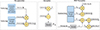 |
Figure 4. Data flow in HQC scheme [25] |
| In the text | |
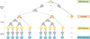 |
Figure 5. The data flow in Sphincs+ scheme [17] |
| In the text | |
 |
Figure 6. The whole data flow in the signature generation process of Rainbow [63] |
| In the text | |
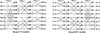 |
Figure 7. The scheme of merged NTT/INTT [31] |
| In the text | |
|
Figure 8. Two different ways to implement NTT hardware |
| In the text | |
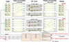 |
Figure 9. The typical data flow in vectorized NTT architecture [31] |
| In the text | |
|
Figure 10. The typical architecture of R2MDC NTT [91] |
| In the text | |
|
Figure 11. The scheme of reconfigurable AE [31] |
| In the text | |
|
Figure 12. Scaling hiding strategy in ref. [31] |
| In the text | |
|
Figure 13. Input and output modules in the Karatsuba scheduling layer [94] |
| In the text | |
|
Figure 14. Efficient Toom-Cook hardware in ref. [96] |
| In the text | |
|
Figure 15. Vectorized-coefficient inversion hardware in ref. [31] |
| In the text | |
|
Figure 16. Dynamic calculating-scheduling framework [115] |
| In the text | |
|
Figure 17. Calculating-scheduling flow and Rd/Wr cases for instruction memories [115] |
| In the text | |
|
Figure 18. Dedicated HQC decapsulation module [98] |
| In the text | |
|
Figure 19. Dedicated BIKE decoding module [118] |
| In the text | |
|
Figure 20. Complete McEliece decoding module [38] |
| In the text | |
|
Figure 21. Round-parallel SHA-3 modules to accelerate Sphincs+ [125] |
| In the text | |
|
Figure 22. 2D array-based matrix inversion hardware [128] |
| In the text | |
|
Figure 23. Reusable array-based matrix inversion hardware [31] |
| In the text | |
|
Figure 24. Efficient Montgomery reduction unit in SIKE hardware [140] |
| In the text | |
|
Figure 25. Tightly-coupled PQC architecture [141] |
| In the text | |
|
Figure 26. FPGA-based HQC accelerator [98] |
| In the text | |
|
Figure 27. FPGA-based Sphincs+ accelerator [124] |
| In the text | |
|
Figure 28. FPGA-based lattice accelerator [36] |
| In the text | |
|
Figure 29. FPGA-based BIKE accelerator [118] |
| In the text | |
|
Figure 30. Kyber-specific ASIC [86] |
| In the text | |
|
Figure 31. Silicon-proven performance comparisons (Throughput vs. Energy efficiency; Throughput vs. Existing Supported Schemes.) |
| In the text | |
|
Figure 32. Dynamically-updated task path in ref. [50] |
| In the text | |
|
Figure 33. The architecture of arithmetic cluster and reconfigurable arithmetic element [50] |
| In the text | |
|
Figure 34. Top-down and bottom up reconfigurability |
| In the text | |
Current usage metrics show cumulative count of Article Views (full-text article views including HTML views, PDF and ePub downloads, according to the available data) and Abstracts Views on Vision4Press platform.
Data correspond to usage on the plateform after 2015. The current usage metrics is available 48-96 hours after online publication and is updated daily on week days.
Initial download of the metrics may take a while.